ADP196 Overview
Description
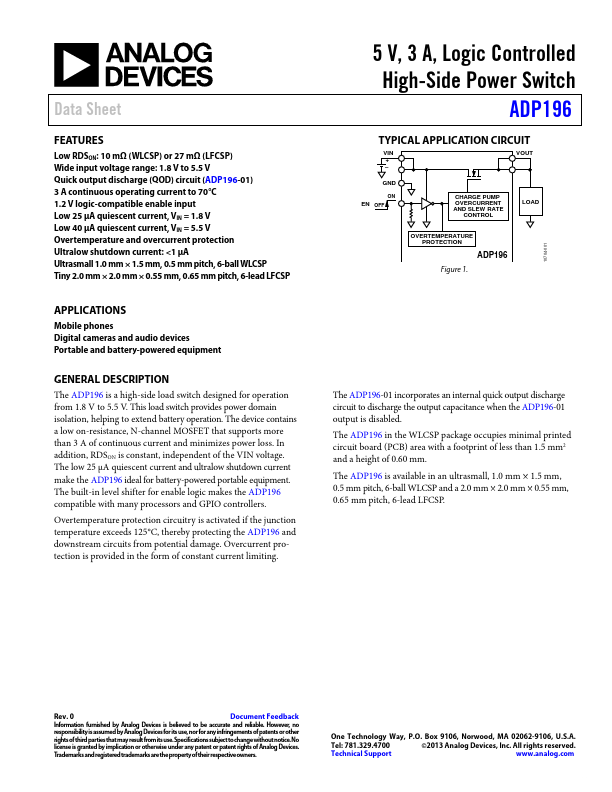
The ADP196 is a high-side load switch designed for operation from 1.8 V to 5.5 V. This load switch provides power domain isolation, helping to extend battery operation.
| Part | ADP196 |
|---|---|
| Description | High-Side Power Switch |
| Manufacturer | Analog Devices |
| Size | 547.53 KB |
The ADP196 is a high-side load switch designed for operation from 1.8 V to 5.5 V. This load switch provides power domain isolation, helping to extend battery operation.
| Part Number | Manufacturer | Description |
|---|---|---|
| SW-331 | Tyco Electronics | Matched GaAs SPDT Switch |
| B3045G | onsemi | Switch-mode Power Rectifiers |
| DK1203 | Dongke Semiconductor | AC-DC Switch Mode Power controller |