ADP198 Overview
Description
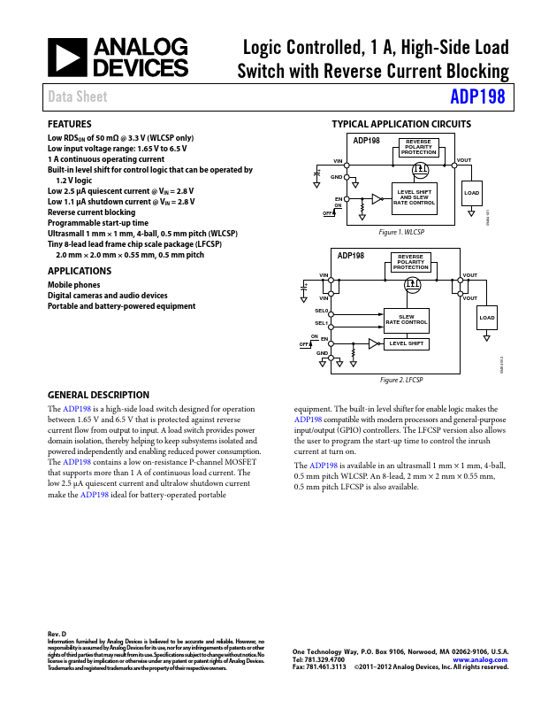
The ADP198 is a high-side load switch designed for operation between 1.65 V and 6.5 V that is protected against reverse current flow from output to input. A load switch provides power domain isolation, thereby helping to keep subsystems isolated and powered independently and enabling reduced power consumption.
Key Features
- Logic Controlled, 1 A, High-Side Load Switch with Reverse Current Blocking ADP198