Analog Devices ADP3161
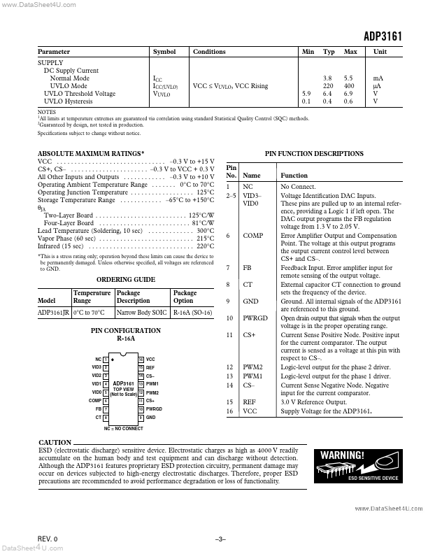
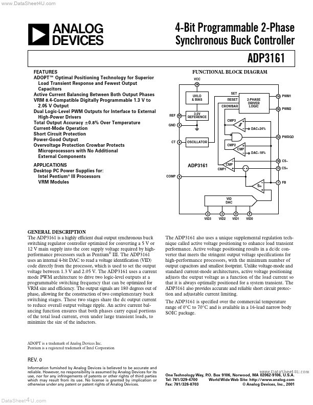
The ADP3161 is a highly efficient dual output synchronous buck switching regulator controller optimized for converting a 5 V or 12 V main supply into the core supply voltage required by highperformance processors such as Pentium® III. The ADP3161 uses an internal 4-bit DAC to read a voltage identification (VID) code directly from the processor, which is used to set the output voltage between 1.3 V and 2.05 V. The ADP3161 uses a current mode PWM architecture to drive two logic-level outputs at a programmable switching frequency that can be optimized for VRM size and efficiency.| Part No. | ADP3161 |
|---|---|
| Datasheet | ADP3161 Download |
| Manufacturer |  Analog Devices |
| Description | 4-Bit Programmable 2-Phase Synchronous Buck Controller |
| Buy | Stock & Price |
FEATURES
ADOPT™ Optimal Positioning Technology for Superior Load Transient Response and Fewest Output Capacitors Active Current Balancing Between Both Output Phases VRM 8.4-Compatible Digitally Programmable 1.3 V to 2.05 V Output Dual Logic-Level PWM Outputs for Interface to External High-Power Drivers Total Output Accuracy ؎0.8% Over Temperature Current-Mode Operation Short Circuit Protection Power-Good Output Overvoltage Protection Crowbar Protects Microprocessors with No Additional External ComponentsAPPLICATIONS
Desktop PC Power Supplies for: Intel Pentium® III Processors VRM Modules 4-Bit Programmable 2-Phase Synchronous Buck Controller ADP3161 FUNCTIONAL BLOCK DIAGRAM VCC UVLO & BIAS SET RESET CROWBAR REF GND DAC+24% PWRGD CT OSCILLATOR CMP2 CMP DAC–18% CS– 3.0V REFERENCE CMP3 2-PHASE DRIVER LOGIC PWM1 PWM2 ADP3161 COMP CMP CMP1 CS+ FB gm VID DAC VID3 VID2 VID1 VID0GENERAL DESCRIPTION
The output signals are 180 degrees out of phase, allowing for the construction of two complementary buck switching stages.