ADV3200
Overview
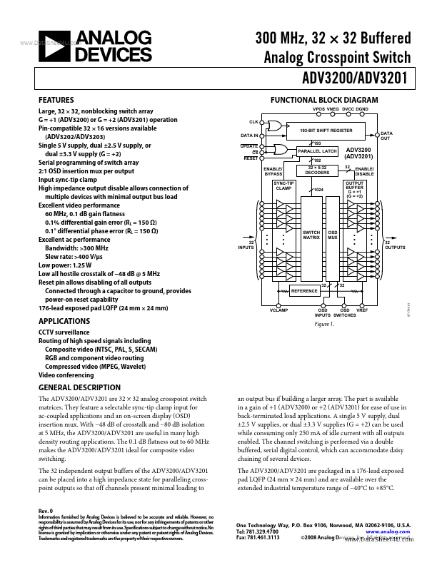
The ADV3200/ADV3201 are 32 × 32 analog crosspoint switch matrices. They feature a selectable sync-tip clamp input for ac-coupled applications and an on-screen display (OSD) insertion mux.
| Part | ADV3200 |
|---|---|
| Description | 32 X 32 Buffered Analog Crosspoint Switch |
| Manufacturer | Analog Devices |
| Size | 1.36 MB |
The ADV3200/ADV3201 are 32 × 32 analog crosspoint switch matrices. They feature a selectable sync-tip clamp input for ac-coupled applications and an on-screen display (OSD) insertion mux.
| Part Number | Manufacturer | Description |
|---|---|---|
| SW-331 | Tyco Electronics | Matched GaAs SPDT Switch |
| B3045G | onsemi | Switch-mode Power Rectifiers |
| DK1203 | Dongke Semiconductor | AC-DC Switch Mode Power controller |