The following content is an automatically extracted verbatim text
from the original manufacturer datasheet and is provided for reference purposes only.
View original datasheet text
www.DataSheet4U.com
300 MHz, 32 × 16 Buffered Analog Crosspoint Switch ADV3202/ADV3203
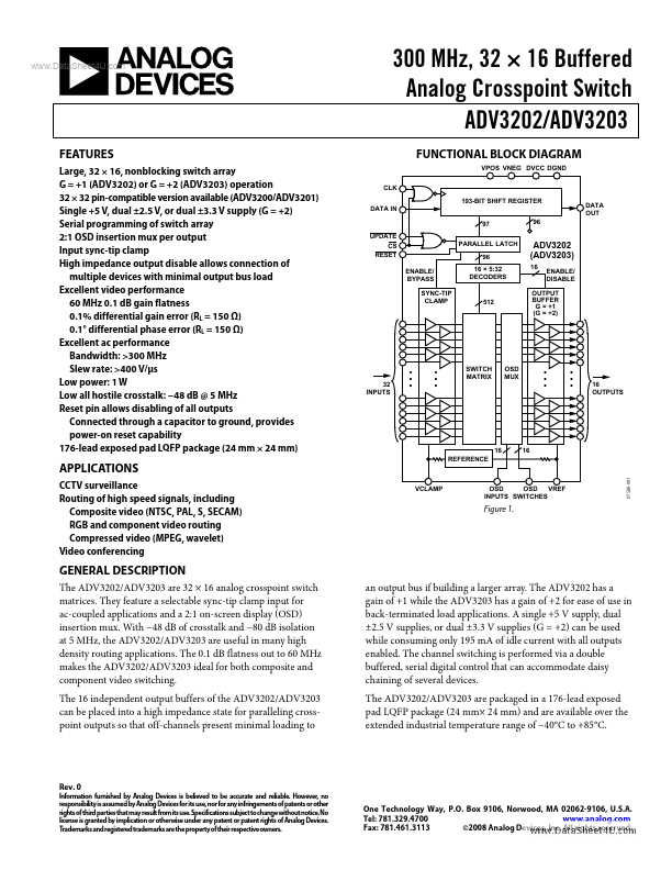
FUNCTIONAL BLOCK DIAGRAM
VPOS VNEG DVCC DGND CLK 193-BIT SHIFT REGISTER DATA IN 97 UPDATE CS RESET ENABLE/ BYPASS SYNC-TIP CLAMP PARALLEL LATCH 96 16 × 5:32 DECODERS 96 DATA OUT
FEATURES
Large, 32 × 16, nonblocking switch array G = +1 (ADV3202) or G = +2 (ADV3203) operation 32 × 32 pin-compatible version available (ADV3200/ADV3201) Single +5 V, dual ±2.5 V, or dual ±3.3 V supply (G = +2) Serial programming of switch array 2:1 OSD insertion mux per output Input sync-tip clamp High impedance output disable allows connection of multiple devices with minimal output bus load Excellent video performance 60 MHz 0.1 dB gain flatness 0.1% differential gain error (RL = 150 Ω) 0.