FEATURES
23 ns or 65 ns Propagation Delay Single-Supply Operation Compatible with 3 V and 5 V Logic Separate Input and Output Sections Low Power Wide Input Range: –5 V to +3.9 V APPLICATIONS
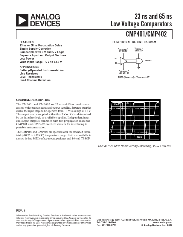
Battery-Operated Instrumentation Line Receivers Level Translators Read Channel Detection 23 ns and 65 ns Low Voltage Comparators CMP401/CMP402 FUNCTIONAL BLOCK DIAGRAM VANALOG+ = 0V OR 5V VDIGITAL = 3V OR 5V IN+ OUTPUT IN– VANALOG– = +0V OR –5V NOTE: (VANALOG+ ) – (VANALOG–) 3V GENERAL DESCRIPTION
Separate supplies enable the input stage to be operated from +3 V to as high as ±6 V. Independent input and output supplies combined with fast propagation make the CMP401 and CMP402 excellent choices for interfacing to portable instrumentation. Both are available in narrow 16-lead SOIC surface-mount packages and 16-lead TSSOP. 50mV 100 90 2v 10 0% 10nS CMP401: 20 MHz Noninverting Switching, VIN = ±100 mV REV. B Information furnished by Analog Devices is believed to be accurate and reliable. However, no re... Analog Devices