CMP402
CMP402 is Low Voltage Comparators manufactured by Analog Devices.
FEATURES
23 ns or 65 ns Propagation Delay Single-Supply Operation patible with 3 V and 5 V Logic Separate Input and Output Sections Low Power Wide Input Range:
- 5 V to +3.9 V
APPLICATIONS Battery-Operated Instrumentation Line Receivers Level Translators Read Channel Detection
23 ns and 65 ns Low Voltage parators
CMP401/CMP402
FUNCTIONAL BLOCK DIAGRAM
VANALOG+ = 0V OR 5V
VDIGITAL = 3V OR 5V
IN+ OUTPUT
IN-
VANALOG- = +0V OR
- 5V
NOTE: (VANALOG+ )
- (VANALOG- ) 3V
GENERAL DESCRIPTION
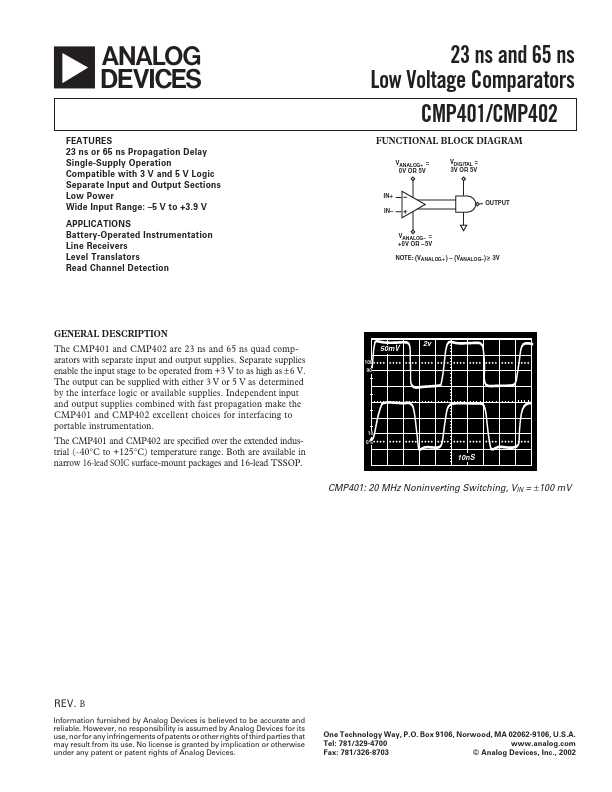
The CMP401 and CMP402 are 23 ns and 65 ns quad parators with separate input and output supplies. Separate supplies enable the input stage to be operated from +3 V to as high as ±6 V. The output can be supplied with either 3 V or 5 V as determined by the interface logic or available supplies. Independent input and output supplies bined with fast propagation make the CMP401 and CMP402 excellent choices for interfacing to portable instrumentation.
The CMP401 and CMP402 are specified over the extended industrial (- 40°C to +125°C) temperature range. Both are available in narrow 16-lead SOIC surface-mount packages and 16-lead TSSOP.
50m V
100 90
2v
10 0%
10n S
CMP401: 20 MHz Noninverting Switching, VIN = ±100 m V
REV. B
Information furnished by Analog Devices is believed to be accurate and reliable. However, no responsibility is assumed by Analog Devices for its use, nor for any infringements of patents or other rights of third parties that may result from its use. No license is granted by implication or otherwise under any patent or patent rights of Analog Devices.
One Technology Way, P.O. Box 9106, Norwood, MA 02062-9106, U.S.A.
Tel: 781/329-4700
.analog.
Fax: 781/326-8703
© Analog Devices, Inc., 2002
CMP401/CMP402- SPECIFICATIONS
ELECTRICAL SPECIFICATIONS (@ V+ANA = V+DIG = 5.0 V, VCM = 0.1 V,
- 40؇C ≤ TA ≤ +125؇C, unless otherwise noted.)
Parameter
Symbol Conditions
Min Typ
Max Unit
INPUT CHARACTERISTICS Offset Voltage1
Hysteresis Input Bias...