FEATURES
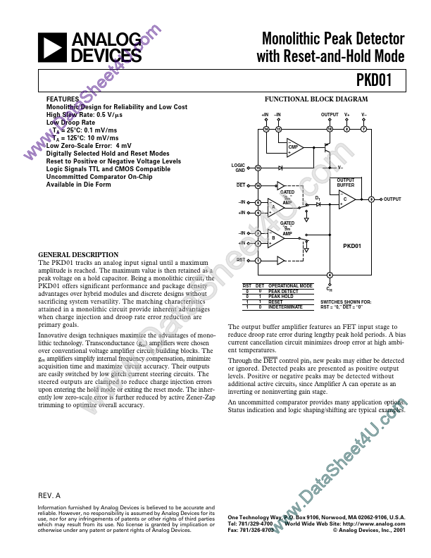
Monolithic Design for Reliability and Low Cost High Slew Rate: 0.5 V/● s Low Droop Rate TA = 25؇ C: 0.1 mV/ms T A = 125؇ C: 10 mV/ms Low Zero-Scale Error: 4 mV Digitally Selected Hold and Reset Modes Reset to Positive or Negative Voltage Levels Logic Signals TTL and CMOS Compatible Uncommitted Comparator On-Chip Available in Die Form w – CMP + LOGIC GND DET GATED "gm" AMP –IN +IN – + –IN +IN GENERAL DESCRIPTION
Being a monolithic circuit, the PKD01 offers significant performance and package density advantages over hybrid modules and discrete designs without sacrificing system versatility. Innovative design techniques maximize the advantages of monolithic technology. Transconductance (gm) amplifiers were chosen over conventional voltage amplifier circuit building blocks. The gm amplifiers simplify internal frequency compensation, minimize acquisition time and maximize circuit accuracy. Their outputs are easily switched by low glitch current steering circuits. The steered outputs are clamped to reduce charge injection errors upon entering the hold mode or exiting the reset mode. Analog Devices