MT5C1008LL
MT5C1008LL is 128K x 8 SRAM WITH DUAL CHIP ENABLE ULTRA LOW POWER manufactured by Austin Semiconductor.
SRAM
Austin Semiconductor, Inc. 128K x 8 SRAM
WITH DUAL CHIP ENABLE ULTRA LOW POWER
AVAILABLE AS MILITARY SPECIFICATIONS
- MIL-STD-883, para. 1.2.2 pliant
MT5C1008(LL) Ultra Low Power
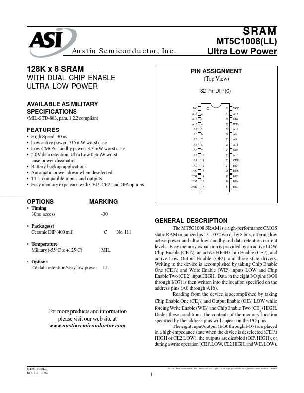
PIN ASSIGNMENT (Top View)
32-Pin DIP (C)
NC A16 A14 A12
1 2 3 4 5 6 7 8 9 10 11 12 13 14 15 16
32 31 30 29 28 26 27 25 24 23 22 21 20 19 18 17
VCC A15 CE2 WE A13 A8 A9 A11 OE A10 CE1 I/O7 I/O6 I/O5 I/O4 I/O3
Features
- -
- -
- -
- -
..
A7 A6 A5 A4 A3 A2 A1 A0 I/O0 I/O1 I/O2 GND
High Speed: 30 ns Low active power: 715 m W worst case Low CMOS standby power: 3.3 m W worst case 2.0V data retention, Ultra Low 0.3m W worst case power dissipation Battery backup applications Automatic power-down when deselected TTL-patible inputs and outputs Easy memory expansion with CE1, CE2, and OE options
OPTIONS
- Timing 30ns access
- Package(s) Ceramic DIP (400 mil)
- Temperature Military (-55°C to +125°C)
MARKING
-30
GENERAL DESCRIPTION
C No. 111 The MT5C1008 SRAM is a high-performance CMOS static RAM organized as 131, 072 words by 8 bits, offering low active power and ultra low standby and data retention current levels. Easy memory expansion is provided by an active LOW Chip Enable (CE1), an active HIGH Chip Enable (CE2), and active Low Output Enable (OE), and three-state drivers. Writing to the device is acplished by taking Chip Enable One (CE1) and Write Enable (WE) inputs LOW and Chip Enable Two (CE2) input HIGH. Data on the eight I/O pins (I/O0 through I/O7) is then written into the location specified on the address pins (A0 through A16). Reading from the device is acplished by taking Chip Enable One (CE1) and Output Enable (OE) LOW while forcing Write Enable (WE) and Chip Enable Two (CE2) HIGH. Under these conditions, the contents of the memory location specified by the address pins will appear on the I/O pins. The eight input/output (I/O0 through I/O7) are placed in a high-impedance state when the device is deselected (CE1) HIGH or CE2 LOW), the outputs are...