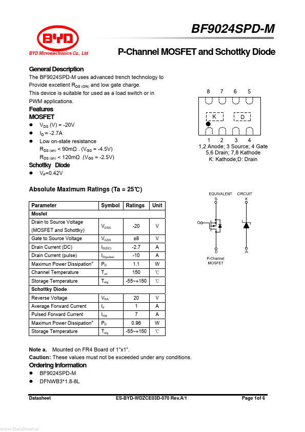
BF9024SPD-M
BF9024SPD-M is P-Channel MOSFET and Schottky Diode manufactured by BYD.
Description
The BF9024SPD-M uses advanced trench technology to Provide excellent RDS (ON) and low gate charge. This device is suitable for used as a load switch or in PWM applications.
Features
MOSFET z z z VDS (V) = -20V ID = -2.7A Low on-state resistance RDS (on) < 90mΩ . (VGS = -4.5V) RDS (on) < 120mΩ .(VGS = -2.5V) VF=0.42V
1 2 3 4 1,2 Anode; 3 Source; 4 Gate 5,6 Drain; 7,8 Kathode K: Kathode;D: Drain
Schottky Diode z
Absolute Maximum Ratings (Ta = 25℃)
Parameter
Mosfet Drain to Source Voltage (MOSFET and Schottky) Gate to Source Voltage Drain Current (DC) Drain Current (pulse) Maximun Power Dissipation Channel Temperature Storage Temperature Schottky Diode Reverse Voltage Average Forward Current Pulsed Forward Current Maximun Power Dissipation Storage Temperature a a
Symbol
Ratings
Unit
VDSS VGSS ID(DC) ID(pulse) PD Tch Tstg VKA IF IFM PD Tstg
-20 ±8 -2.7 -10 1.1 150 -55~+150 20 1 7 0.96 -55~+150
V V A A W ℃ ℃ V A A W ℃
Note a. Mounted on FR4 Board of 1”x1”. Caution: These values must not be exceeded under any conditions.
Ordering Information z z BF9024SPD-M DFNWB3- 1.8-8L
ES-BYD-WDZCE03D-070 Rev.A/1 Page 1of 6
.Data Sheet.in
BYD Microelectronics Co., Ltd.
Electrical Characteristics (TC = 25℃)
Characteristic
Mosfet
Symbol
IDSS IGSS VGS(th) |yfs| RDS(on)
Ciss Coss Crss
Test Conditions
VDS= -20V,VGS=0V VGS= ± 8V,VDS=0V VDS=VGS,ID=
- 0.25m A VDS= -10V, ID= -2A VGS= -4.5V,ID= -2A VGS= -2.5V,ID= -2A VDS= -10V ,VGS =0,f=1MHZ VDS= -10V, ID= -1A, VGS= -4.5V, RG=6Ω VDS= -10V, VGS= -4.5V, ID= -2A IF=-0.9A,VGS=0V IF=0.5A Vr=20V Vr=10V
Min.
- Typ.
- Max.
-1 ±100 -1
-...