BF92301P
Description
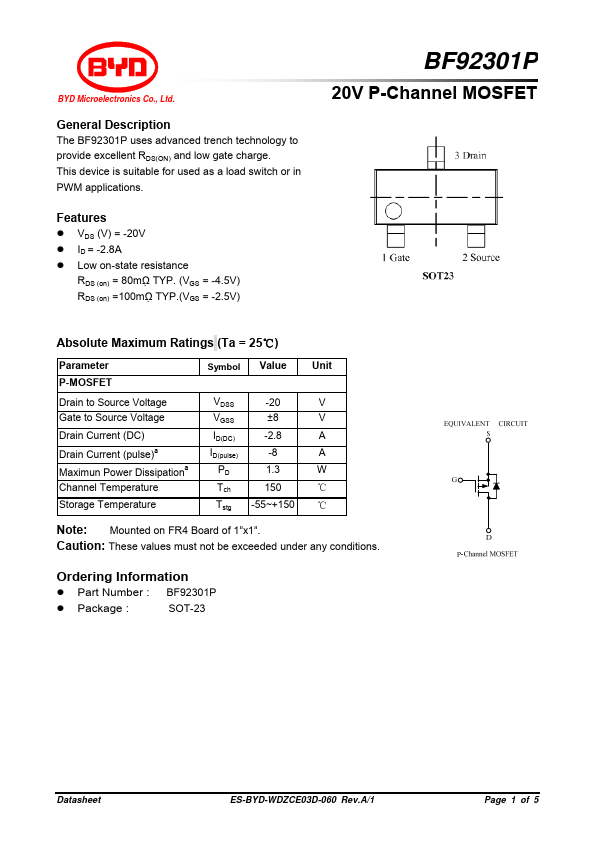
The BF92301P uses advanced trench technology to provide excellent RDS(ON) and low gate charge. This device is suitable for used as a load switch or in PWM applications.
The BF92301P uses advanced trench technology to provide excellent RDS(ON) and low gate charge. This device is suitable for used as a load switch or in PWM applications.