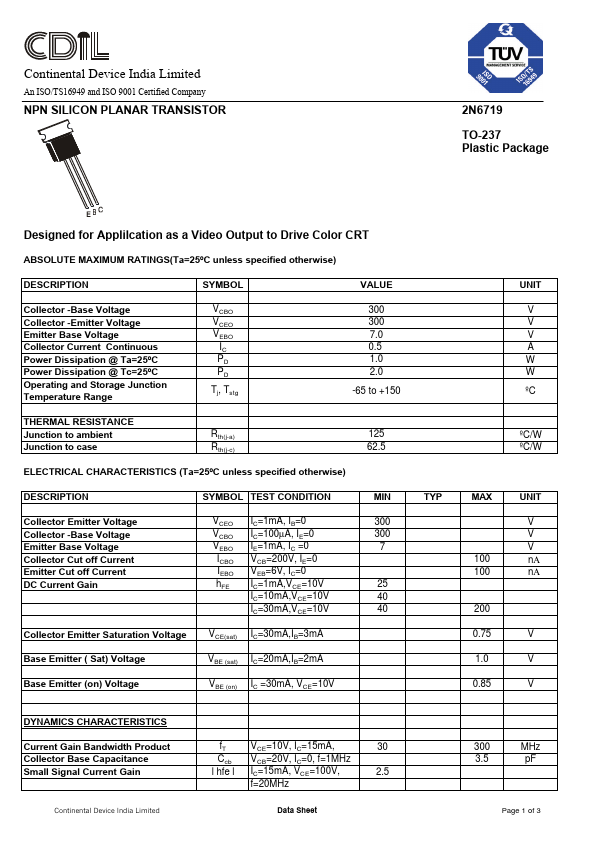
ABSOLUTE MAXIMUM RATINGS
(Ta=25ºC unless specified otherwise) DESCRIPTION
SYMBOL VALUE Collector -Base Voltage Collector -Emitter Voltage Emitter Base Voltage Collector Current Continuous Power Dissipation @ Ta=25ºC Power Dissipation @ Tc=25ºC Operating and Storage Junction Temperature Range VCBO VCEO VEBO IC PD PD Tj, Tstg 300 300 7.0 0.5 1.0 2.0 -65 to +150 THERMAL RESISTANCE Junction to ambient Junction to case Rth(j-a) Rth(j-c) ELECTRICAL CHARACTERISTICS
(Ta=25ºC unless specified otherwise) 125 62.5 DESCRIPTION
SYMBOL TEST CONDITION MIN Collector Emitter Voltage Collector -Base Voltage Emitter Base Voltage Collector Cut off Current Emitter Cut off Current DC Current Gain Collector Emitter Saturation Voltage Base Emitter ( Sat) Voltage Base Emitter (on) Voltage VCEO VCBO VEBO ICBO IEBO hFE IC=1mA, IB=0 IC=100µA, IE=0 IE=1mA, IC =0 VCB=200V, IE=0 VEB=6V, IC=0 IC=1mA,VCE=10V IC=10mA,VCE=10V IC=30mA,VCE=10V VCE(sat) IC=30mA,IB=3mA VBE (sat) IC=20mA,IB=2mA VBE (on) IC =30mA, VCE=10V 300... Continental Device India