• Part: CEB540A
  • Description: N-Channel MOSFET
  • Category: MOSFET
  • Manufacturer: CET
  • Size: 103.90 KB
Download CEB540A Datasheet PDF
CET
CEB540A
CEB540A is N-Channel MOSFET manufactured by CET.
FEATURES 100V, 36A, RDS(ON) = 48mΩ @VGS = 10V. Super high dense cell design for extremely low RDS(ON). High power and current handing capability. Lead free product is acquired. 
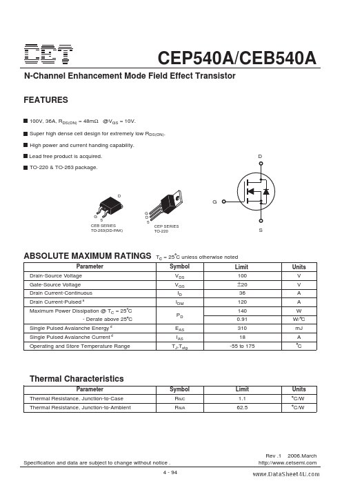
TO-220 & TO-263 package. D S CEB SERIES TO-263(DD-PAK) G CEP SERIES TO-220 ABSOLUTE MAXIMUM RATINGS Parameter Drain-Source Voltage Gate-Source Voltage Drain Current-Continuous Drain Current-Pulsed a Tc = 25 C unless otherwise noted Symbol Limit VDS VGS ID IDM PD EAS IAS TJ,Tstg 100 Units V V A A W W/ C m J A C ±20 36 120 140 0.91 310 18 -55 to 175 Maximum Power Dissipation @ TC = 25 C - Derate above 25 C Single Pulsed Avalanche Energy d Single Pulsed Avalanche Current d Operating and Store Temperature Range Thermal Characteristics Parameter Thermal Resistance, Junction-to-Case Thermal Resistance, Junction-to-Ambient Symbol RθJC RθJA Limit 1.1 62.5 Units C/W C/W Specification and data are subject to change without notice . 4 - 94 Rev .1 2006.March http://.cetsemi. CEP540A/CEB540A Electrical Characteristics Parameter Off Characteristics Drain-Source Breakdown Voltage Zero Gate Voltage Drain Current Gate Body Leakage Current, Forward Gate Body Leakage Current, Reverse On Characteristics b Gate Threshold Voltage Static Drain-Source On-Resistance Dynamic Characteristics c Forwand Transconductance Input Capacitance Output Capacitance Reverse Transfer Capacitance Switching Characteristics c Turn-On Delay Time Turn-On Rise Time Turn-Off Delay Time Turn-Off Fall Time Total Gate Charge Gate-Source Charge Gate-Drain Charge Drain-Source Diode Forward Current Drain-Source Diode Forward Voltage b td(on) tr td(off) tf Qg Qgs Qgd IS VSD VGS = 0V, IS = 18A VDS = 80V, ID = 18A, VGS = 10V VDD = 50V, ID = 18A, VGS = 10V, RGEN = 5.1Ω 13 11 32 15 37.5 6 18 36 1.3 40 35 65 45 48 ns ns ns ns n C n C n C A V g FS Ciss Coss Crss VDS = 25V, ID = 18A VDS = 25V, VGS = 0V, f = 1.0 MHz 14 832 240 105 S p F p F p F VGS(th) RDS(on) VGS = VDS, ID = 250µA VGS = 10V, ID = 18A 2 40 4 48 V mΩ BVDSS IDSS IGSSF...