CED20P10
CED20P10 is P-Channel MOSFET manufactured by CET.
CED20P10/CEU20P10
P-Channel Enhancement Mode Field Effect Transistor
PRELIMINARY
Features
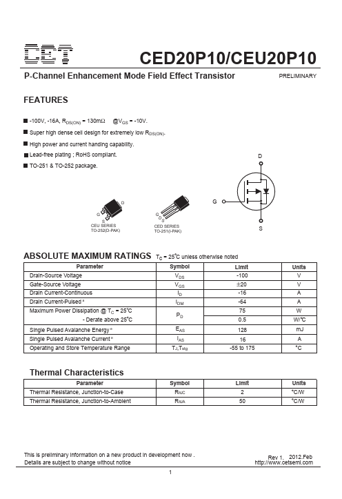
-100V, -16A, RDS(ON) = 130mΩ @VGS = -10V. Super high dense cell design for extremely low RDS(ON). High power and current handing capability. Lead-free plating ; RoHS pliant. TO-251 & TO-252 package.
CEU SERIES TO-252(D-PAK)
G DS
CED SERIES...