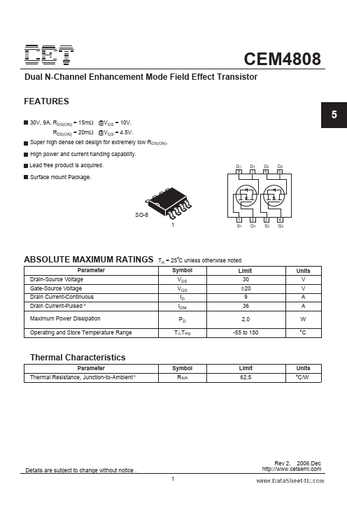
CEM4808 Description
Dual N-Channel Enhancement Mode Field Effect Transistor.
CEM4808 is Dual N-Channel Enhancement Mode Field Effect Transistor manufactured by CET.
| Part Number | Description |
|---|---|
| CEM4804A | Dual N-Channel MOSFET |
| CEM4063 | p- |
| CEM4201 | p- |
| CEM4207 | p- |
| CEM4228 | Dual N-Channel Enhancement Mode Field Effect Transistor |
Dual N-Channel Enhancement Mode Field Effect Transistor.