CET6601 Overview
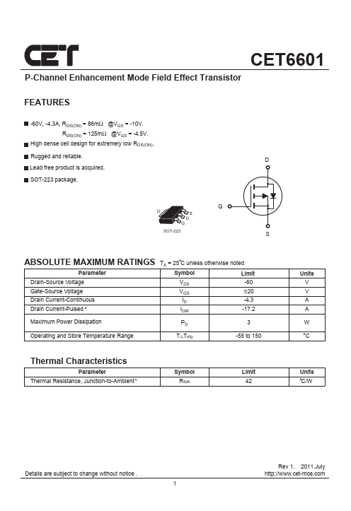
CET6601 P-Channel Enhancement Mode Field Effect Transistor.
CET6601 Key Features
- 60V, -4.3A, RDS(ON) = 86mΩ @VGS = -10V. RDS(ON) = 125mΩ @VGS = -4.5V
CET6601 datasheet by CET.
| Part number | CET6601 |
|---|---|
| Datasheet | CET6601-CET.pdf |
| File Size | 363.38 KB |
| Manufacturer | CET |
| Description | P-Channel MOSFET |
|
|
CET6601 P-Channel Enhancement Mode Field Effect Transistor.
| Part Number | Description |
|---|---|
| CET01N65A | N-Channel MOSFET |
| CET0215 | N-Channel MOSFET |
| CET3301 | P-Channel MOSFET |