3426B
DESCRIPTION
The uses advanced trench technology to provide excellent RDS(ON) and low gate charge. This device is suitable for use as a load switch or in PWM applications.
GENERAL FEATURES
- RDS(ON) < Ω @ VGS=4.5V
RDS(ON) < Ω @ VGS=10V
- High Power and current handing capability
- Lead free product is acquired
- Surface Mount Package
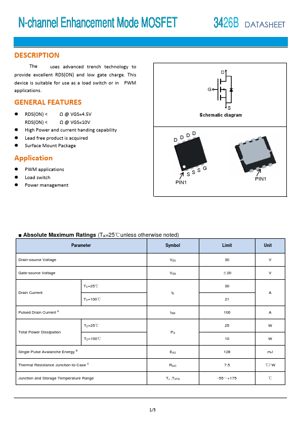
D D DD
Application
- PWM applications
- Load switch
- Power management
SSSG
PIN1
PIN1
- Absolute Maximum Ratings (TA=25℃unless otherwise noted)
Parameter
Symbol
Drain-source Voltage
Gate-source Voltage
Drain Current
TC=25℃ TC=100℃
Pulsed Drain Current A
Total Power Dissipation
TC=25℃
TC=100℃
Single Pulse Avalanche Energy B
Thermal Resistance Junction-to-Case C
Junction and Storage Temperature Range
VDS...