3429DE
DESCRIPTION
The uses advanced trench technology to provide excellent RDS(ON) and low gate charge. This device is suitable for use as a load switch or in PWM applications.
GENERAL FEATURES
- VDS
- ID
- RDS(ON)( at VGS=-4.5V)
- RDS(ON)( at VGS=-2.5V)
- RDS(ON)( at VGS=-1.8V)
-20V -30A <19 mohm <26 mohm <45 mohm
- Trench Power LV MOSFET technology
- High density cell design for Low RDS(ON)
- High Speed switching
Application
- PWM applications
- Load switch
- Power management
3429DE DATASHEET
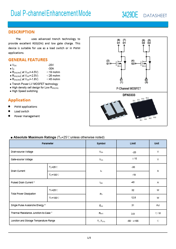
(8) (7) D1 D1
(6) (5) D2 D2
(2) (4) G1 G2
S1 S2 (1) (3)
P-Channel MOSFET
DFN3333
- Absolute Maximum Ratings (TA=25℃unless otherwise noted)
Parameter
Symbol
Drain-source Voltage
Gate-source Voltage
Drain Current Pulsed Drain Current A
TC=25℃ TC=100℃
Total Power Dissipation
TC=25℃ TC=100℃
Single Pulse Avalanche Energy B
Thermal Resistance Junction-to-Case C
Junction and Storage Temperature Range
VDS VGS
EAS RθJC TJ...