Datasheet4U.com
🌙
BSS84N3
BSS84KS3
BSS84N3 Datasheet | CYStech Electronics
Part:
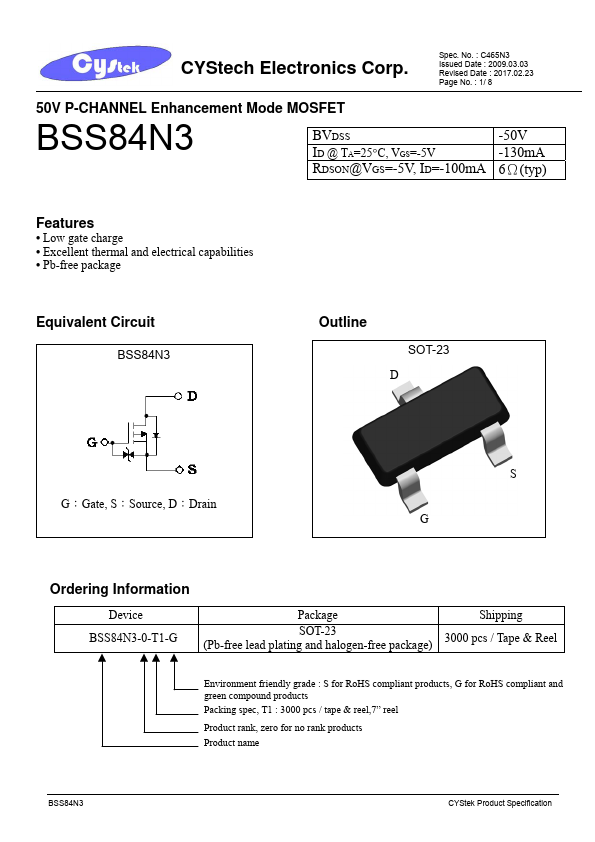
BSS84N3
Description:
50V P-CHANNEL MOSFET
Category:
MOSFET
Manufacturer:
CYStech Electronics
Size:
281.84 KB
BSS84N3 Datasheet (PDF) Download
CYStech Electronics
BSS84N3
Overview
Low gate charge
Excellent thermal and electrical capabilities
Pb-free package
Datasheets by Manufacturer
BSS84ZT
— Unisonic Technologies — P-Channel MOSFET
BSS84
— WEITRON — Small Signal MOSFET
BSS84
— LITEON — P-Channel MOSFET
BSS84DW
— Bruckewell Technology — P-Channel Enhancement Mode MOSFET
×
Close
This website uses cookies or similar technologies, to enhance your browsing experience and provide personalized recommendations.
By continuing to use our website, you agree to our
Privacy Policy
Accept