CYStech Electronics MTN6515E3
N-Channel Logic Level Enhancement Mode Power MOSFET
| Part No. | MTN6515E3 |
|---|---|
| Datasheet | MTN6515E3 Download |
| Manufacturer |  CYStech Electronics |
| Description | N-Channel Logic Level Enhancement Mode Power MOSFET |
| Buy | Stock & Price |
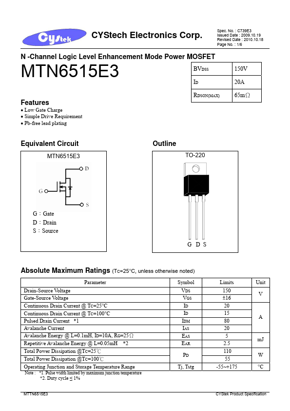
FEATURES
● Low Gate Charge● Simple Drive Requirement
● Pb-free lead plating BVDSS ID RDSON(MAX) 150V 20A 65mΩ Equivalent Circuit MTN6515E3 Outline TO-220 G:Gate D:Drain S:Source G D S
ABSOLUTE MAXIMUM RATINGS
(TC=25°C, unless otherwise noted) Parameter Drain-Source Voltage Gate-Source Voltage Continuous Drain Current @ TC=25°C Continuous Drain Current @ TC=100°C Pulsed Drain Current *1 Avalanche Current Avalanche Energy @ L=0.1mH, ID=10A, RG=25Ω Repetitive Avalanche Energy @ L=0.05mH *2 Total Power Dissipation @TC=25℃ Total Power Dissipation @TC=100℃ Operating Junction and Storage Temperature Range Note : *1. Pulse width limited by maximum junction temperature Symbol VDS VGS ID ID IDM IAS EAS EAR PD Tj, Tstg Limits 150 ±16 20 15 80 20 5 2.5 110 55 -55~+175 Unit V A mJ W °C *2. Duty cycle ≤ 1% MTTN6515E3 CYStek Product Specification CYStech Electronics Corp. Thermal Data Parameter Thermal Resistance, Junction-to-case, max Thermal Resistance, Junction-to-ambient, max Symbol Rth,j-c Rth,j-a Spec.