MTN6515J3
MTN6515J3 is N-Channel Logic Level Enhancement Mode Power MOSFET manufactured by CYStech Electronics.
CYStech Electronics Corp.
N -Channel Logic Level Enhancement Mode Power MOSFET
Spec. No. : C739J3 Issued Date : 2009.10.19 Revised Date : 2013.12.25 Page No. : 1/9
Features
- Low Gate Charge
- Simple Drive Requirement
- Pb-free lead plating and halogen-free package
BVDSS 150V ID RDS(ON)@VGS=10V, ID=15A RDS(ON)@VGS=5V, ID=10A RDS(ON)@VGS=3V, ID=3A
20A 60mΩ(typ) 59mΩ(typ) 60mΩ(typ)
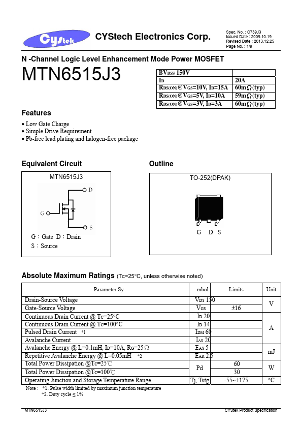
Equivalent Circuit
Outline
TO-252(DPAK)
G:Gate D:Drain...