Datasheet4U.com
🌙
MTP3J15N3 Datasheet | CYStech Electronics
Part:
MTP3J15N3
Description:
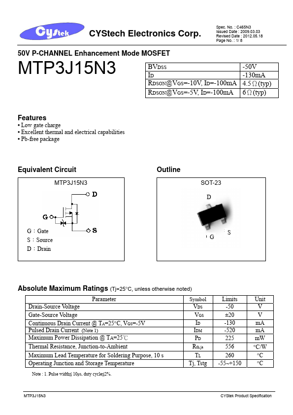
50V P-CHANNEL Enhancement Mode MOSFET
Category:
MOSFET
Manufacturer:
CYStech Electronics
Size:
346.63 KB
MTP3J15N3 Datasheet (PDF) Download
Related MTP3J15N3 Datasheets
MTP3J15Y3 50V P-CHANNEL Enhancement Mode MOSFET
CYStech Electronics
MTP3J15N3
Key Features
Low gate charge
Excellent thermal and electrical capabilities
Pb-free package
50V -130mA 4.5Ω(typ) 6Ω(typ)
×
Close