CYStech Electronics MTP3LP01Y3
30V P-CHANNEL Enhancement Mode MOSFET
| Part No. | MTP3LP01Y3 |
|---|---|
| Datasheet | MTP3LP01Y3 Download |
| Manufacturer |  CYStech Electronics |
| Description | 30V P-CHANNEL Enhancement Mode MOSFET |
| Buy | Stock & Price |
FEATURES
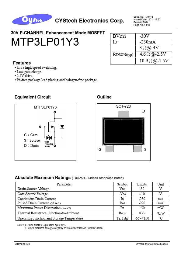
● Ultra high speed switching.● Low gate charge.
● 2.5V drive.
● Pb-free package lead plating and halogen-free package. BVDSS ID RDSON(typ) -30V -230mA 3Ω@-4V 4.6Ω@-2.5V 10.9Ω@-1.5V Equivalent Circuit MTP3LP01Y3 Outline SOT-723 D G:Gate S:Source D:Drain G S
ABSOLUTE MAXIMUM RATINGS
(Ta=25°C, unless otherwise noted) Parameter Drain-Source Voltage Gate-Source Voltage Continuous Drain Current Pulsed Drain Current (Note 1) Maximum Power Dissipation (Note 2) Thermal Resistance, Junction-to-Ambient Operating Junction and Storage Temperature Note : 1. Pulse width≤ 10μs, duty cycle≤1%. 2. When mounted on a glass epoxy with a dimension of 100mm²×1mm. Symbol VDS VGS ID IDM PD Rth,ja Tj, Tstg Limits -30 ±10 -230 -920 150 833 -55~+150 Unit V V mA mA mW °C/W °C MTP3LP01Y3 CYStek Product Specification CYStech Electronics Corp.ELECTRICAL CHARACTERISTICS
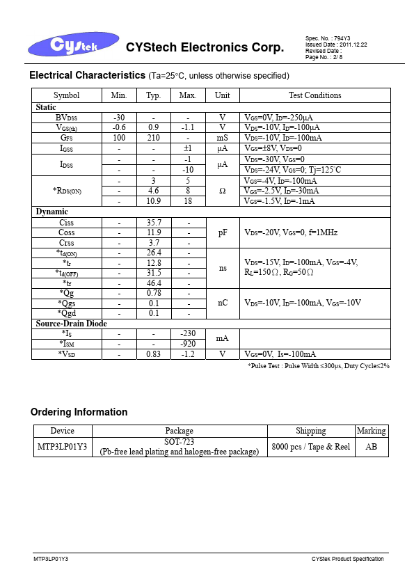
(Ta=25°C, unless otherwise specified) Symbol Static BVDSS VGS(th) GFS IGSS IDSS *RDS(ON) Dynamic Ciss Coss Crss *td(ON) *tr *td(OFF) *tf *Qg *Qgs *Qgd Source-Drain Diode *IS *ISM *VSD Min. -30 -0.6 100 Typ.