SST4117
SST4117 is N-Channel JFET General Purpose Amplifier manufactured by Calogic.
FEATURES
Leakage
- Low
- Low Capacitance
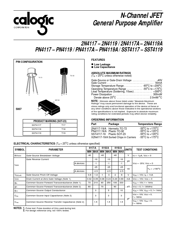
- 92
TO-72
ABSOLUTE MAXIMUM RATINGS (TA = 25o C unless otherwise noted) Gate-Source or Gate-Drain Voltage
- -
- . -40V Gate Current
- -
- -
- - . . . 50m A Storage Temperature Range
- - . . . -65o C to +200o C Operating Temperature Range
- - . -55o C to +175o C Lead Temperature (Soldering, 10sec)
- - . . . +300o C Power Dissipation
- -
- -
- . . . 300m W Derate above 25o C
- -
- - . . . 2.0m W/ o C
NOTE: Stresses above those listed under "Absolute Maximum Ratings" may cause permanent damage to the device. These are stress ratings only and functional operation of the device at these or any other conditions above those indicated in the operational sections of the specifications is not implied. Exposure to absolute maximum rating conditions for extended periods may affect device reliability.
SOT-23 G
PRODUCT MARKING (SOT-23) SST4117 SST4118 SST4119 T17 T18 T19
ORDERING INFORMATION Part Package Temperature Range -55o C to +175o C -55o C to +135o C -55o C to +135o C -55o C to +175o C 2N4117-19/A Hermetic TO-72 PN4117-19/A Plastic TO-92 SST4117-19 Plastic SOT-23 X2N4117-19/A Sorted Chips in Carriers
ELECTRICAL CHARACTERISTICS (TA = 25o C unless otherwise specified)
SYMBOL BVGSS PARAMETER Gate-Source Breakdown Voltage Gate Reverse Current IGSS A devices A devices VGS(off) IDSS gfs gfs gos Ciss Crss Gate-Source Pinch-Off Voltage Drain Current at Zero Gate Voltage (Note 1) mon-Source Forward Transconductance (Note 1) mon-Source Forward Transconductance (Note 2) mon-Source Output Conductance mon-Source Input Capacitance (Note 2) mon-Source Reverse Transfer Capacitance (Note 2) -0.6 70 60 3 3 1.5 4117/A -40 -10 -1 -25 -2.5 -1.8 210 -1 80 70 5 3 1.5 4118/A -40 -10 -1 -25 -2.5 -3 250 -2 100 90 10 3 p F 1.5 4119/A -40 -10 -1 -25 -2.5...