FEATURES
I Fast mode I2C bus compatible* I Max clock frequency: I Industrial and extended temperature ranges I 5 ms max write cycle time I Write protect feature I 1,000,000 program/erase cycles I 100 year data retention - 400KHz for VCC=2.5V to 5.5V I Schmitt trigger filtered inputs for noise suppression I Low power CMOS technology I 64-byte page write buffer I Self-timed write cycle with auto-clear – entire array protected when WP at VIH I 8-pin DIP, 8-pin SOIC (JEDEC), 8-pin SOIC (EIAJ), 8-pin TSSOP and TDFN packages DESCRIPTION
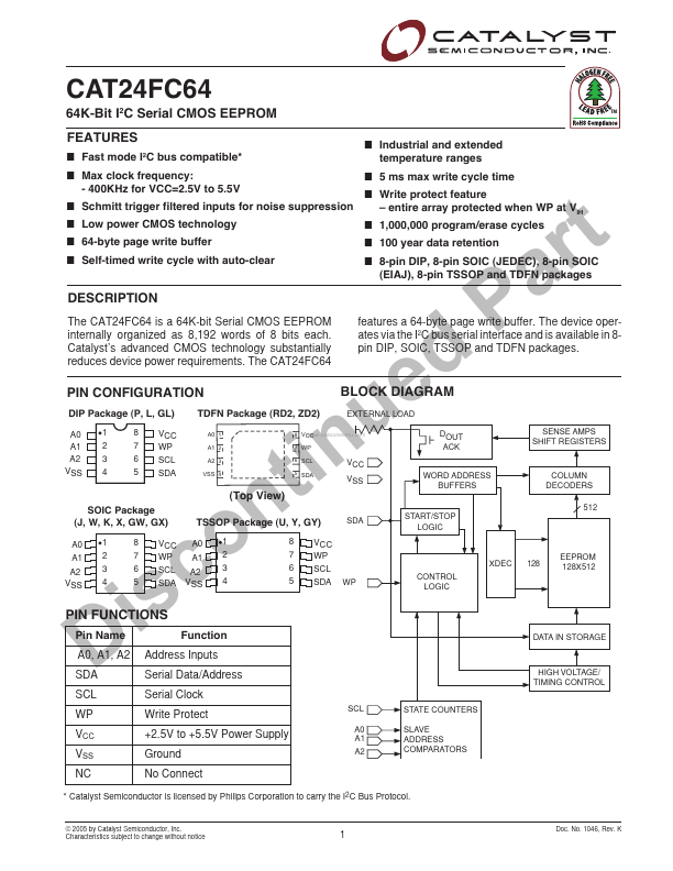
Catalyst’s advanced CMOS technology substantially reduces device power requirements. PIN CONFIGURATION DIP Package (P, L, GL) A0 A1 A2 VSS 1 2 3 4 8 7 6 5 VCC WP SCL SDA TDFN Package (RD2, ZD2) A0 1 A1 2 A2 3 VSS 4 SOIC Package (J, W, K, X, GW, GX) A0 A1 A2 VSS PIN FUNCTIONS Pin Name A0, A1, A2 SDA SCL WP VCC VSS NC s i D 2 3 4 7 6 5 1 8 VCC A0 WP A1 SCL A2 SDA VSS o c 1 2 3 4 (Top View) TSSOP Package (U, Y, GY) 8 7 6 5 i t n 7 WP 6 SCL 5 SDA 8 VCC u n VCC VS... Catalyst Semiconductor