CP219
Overview
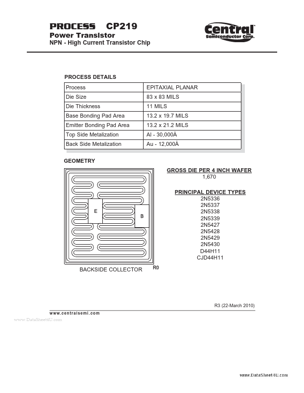
PROCESS Power Transistor CP219 NPN - High Current Transistor Chip PROCESS DETAILS Process Die Size Die Thickness Base Bonding Pad Area Emitter Bonding Pad Area Top Side Metalization Back Side Meta...
| Part | CP219 |
|---|---|
| Description | Power Transistor NPN - High Current Transistor Chip |
| Category | Transistor |
| Manufacturer | Central Semiconductor |
| Size | 759.39 KB |
PROCESS Power Transistor CP219 NPN - High Current Transistor Chip PROCESS DETAILS Process Die Size Die Thickness Base Bonding Pad Area Emitter Bonding Pad Area Top Side Metalization Back Side Meta...
| Part Number | Manufacturer | Description |
|---|---|---|
| CP2102 | Silicon Labs | SINGLE-CHIP USB TO UART BRIDGE |
| CP2102N | Silicon Labs | USB-to-UART bridge controller |
| CP2112 | Silicon Labs | Single-Chip HID USB to SMBus Master Bridge |
| CP2101 | Silicon Labs | Single-Chip USB to UART Bridge |
| CP2129 | CHIP | White LED Step-up Converter |