CP207
CP207 is Small Signal Transistor NPN - Saturated Switch Transistor Chip manufactured by Central Semiconductor.
PROCESS
Small Signal Transistor
- Saturated Switch Transistor Chip
Central
Semiconductor Corp.
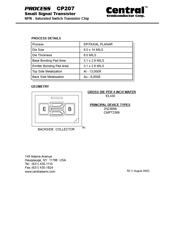
PROCESS DETAILS Process Die Size Die Thickness Base Bonding Pad Area Emitter Bonding Pad Area Top Side Metalization Back Side Metalization GEOMETRY GROSS DIE PER 4 INCH WAFER 93,430 PRINCIPAL DEVICE TYPES 2N2369A CMPT2369 EPITAXIAL PLANAR 9.0 x 14 MILS 8.0 MILS 3.1 x 2.9 MILS 3.1 x 2.9 MILS Al
- 13,000Å Au
- 6,000Å
BACKSIDE COLLECTOR
145 Adams Avenue Hauppauge, NY 11788 USA Tel: (631) 435-1110 Fax: (631) 435-1824 .centralsemi.
R2 (1-August 2002)
Central
PROCESS
Semiconductor Corp.
Typical Electrical Characteristics
145 Adams Avenue Hauppauge, NY 11788 USA Tel: (631) 435-1110 Fax: (631) 435-1824 .centralsemi.
R2 (1-August...