CEB6030LS2
CEB6030LS2 is N-Channel Logic Level Enhancement Mode Field Effect Transistor manufactured by Chino-Excel Technology.
- Part of the CEB6030LS2_Chino comparator family.
- Part of the CEB6030LS2_Chino comparator family.
FEATURES
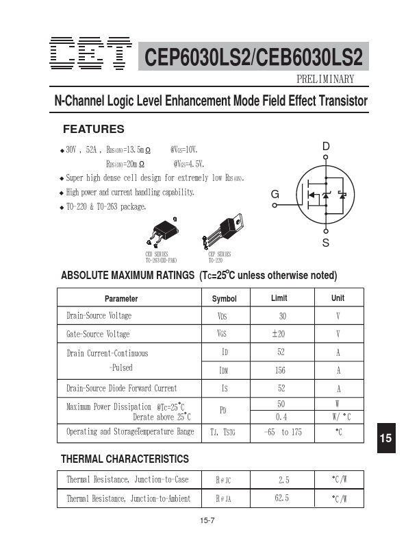
30V , 52A , RDS(ON)=13.5m Ω
@VGS=10V.
RDS(ON)=20m Ω
@VGS=4.5V.
Super high dense cell design for extremely low RDS(ON).
High power and current handling capability.
TO-220 & TO-263 package.
CEB SERIES TO-263(DD-PAK)
CEP SERIES TO-220
ABSOLUTE MAXIMUM RATINGS (TC=25 C unless otherwise noted)
Parameter Drain-Source Voltage
Gate-Source Voltage
Drain Current-Continuous -Pulsed
Drain-Source Diode Forward Current
Maximum Power Dissipation @Tc=25 C Derate above 25 C
Operating and Storage Temperature Range
Symbol VDS VGS ID IDM IS
TJ, TSTG
Limit
Ć20
156 52 50 0.4 -65 to 175
Unit
A A A W W/ C C
THERMAL CHARACTERISTICS
Thermal Resistance, Junction-to-Case Thermal Resistance, Junction-to-Ambient
RįJC RįJA
15-7
2.5 62.5
C /W C...