Datasheet4U Logo Datasheet4U.com

CEM4539 - Dual Enhancement Mode Field Effect Transistor(N and P Channel)

Download the CEM4539 datasheet PDF (CEM4539_Chino included). The manufacturer datasheet provides complete specifications, pinout details, electrical characteristics, and typical applications for dual enhancement mode field effect transistor(n and p channel).

Features

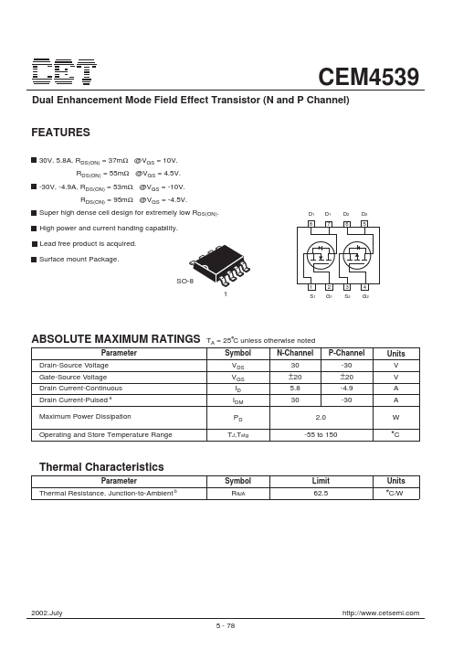
  • 30V, 5.8A, RDS(ON) = 37mΩ @VGS = 10V. RDS(ON) = 55mΩ @VGS = 4.5V. -30V, -4.9A, RDS(ON) = 53mΩ @VGS = -10V. RDS(ON) = 95mΩ @VGS = -4.5V. Super high dense cell design for extremely low RDS(ON). High power and current handing capability. Lead free product is acquired. Surface mount Package. SO-8 1 D1 D1 D2 D2 87 65 1234 S1 G1 S2 G2.

📥 Download Datasheet

Note: The manufacturer provides a single datasheet file (CEM4539_Chino-ExcelTechnology.pdf) that lists specifications for multiple related part numbers.

Datasheet Details

Part number CEM4539
Manufacturer Chino-Excel Technology
File Size 95.30 KB
Description Dual Enhancement Mode Field Effect Transistor(N and P Channel)
Datasheet download datasheet CEM4539 Datasheet
Other Datasheets by Chino-Excel Technology

Full PDF Text Transcription

Click to expand full text
CEM4539 Dual Enhancement Mode Field Effect Transistor (N and P Channel) FEATURES 30V, 5.8A, RDS(ON) = 37mΩ @VGS = 10V. RDS(ON) = 55mΩ @VGS = 4.5V. -30V, -4.9A, RDS(ON) = 53mΩ @VGS = -10V. RDS(ON) = 95mΩ @VGS = -4.5V. Super high dense cell design for extremely low RDS(ON). High power and current handing capability. Lead free product is acquired. Surface mount Package. SO-8 1 D1 D1 D2 D2 87 65 1234 S1 G1 S2 G2 ABSOLUTE MAXIMUM RATINGS TA = 25 C unless otherwise noted Parameter Symbol N-Channel Drain-Source Voltage Gate-Source Voltage Drain Current-Continuous Drain Current-Pulsed a VDS 30 VGS ±20 ID 5.8 IDM 30 P-Channel -30 ±20 -4.9 -30 Maximum Power Dissipation PD 2.
Published: |