Datasheet Summary
N-Channel Enhancement Mode Field Effect Transistor
Features
30V, 10A, RDS(ON) = 15mΩ @VGS = 10V. RDS(ON) = 20mΩ @VGS = 4.5V.
Super high dense cell design for extremely low RDS(ON). High power and current handing capability. Lead free product is acquired. Surface mount Package.
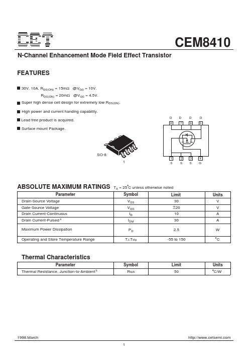
DD D D 8 7 65
SO-8
1 234 S...