CEP04N6
CEP04N6 is N-Channel Logic Level Enhancement Mode Field Effect Transistor manufactured by Chino-Excel Technology.
- Part of the CEP04N6_Chino comparator family.
- Part of the CEP04N6_Chino comparator family.
FEATURES
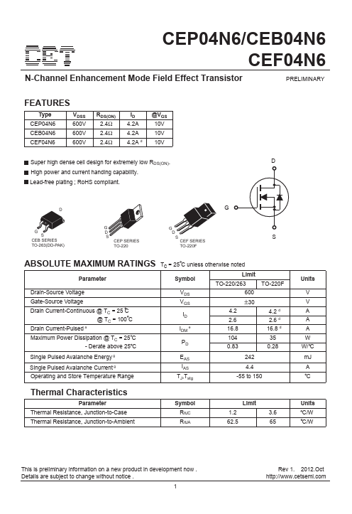
Type CEP04N6 CEB04N6 CEF04N6
VDSS 600V 600V
600V
RDS(ON) 2.4Ω 2.4Ω
2.4Ω
ID 4.2A 4.2A 4.2A d
@VGS 10V 10V
10V
Super high dense cell design for extremely low RDS(ON). High power and current handing capability. Lead-free plating ; Ro HS pliant.
CEB SERIES TO-263(DD-PAK)
CEP SERIES TO-220
D S CEF SERIES
TO-220F
ABSOLUTE MAXIMUM RATINGS
Parameter
Drain-Source Voltage Gate-Source Voltage Drain Current-Continuous @ TC = 25 C
@ TC = 100 C Drain Current-Pulsed a Maximum Power Dissipation @ TC = 25 C
- Derate above 25 C
Tc = 25 C unless otherwise noted
Symbol
Limit TO-220/263
VDS 600
VGS ±30
4.2 2.6
IDM e
104 PD 0.83
TO-220F
4.2 d 2.6 d 16.8 d 35 0.28
Single Pulsed Avalanche Energy g
Single Pulsed Avalanche Current g Operating and Store Temperature Range
EAS IAS...