CEU93A3
CEU93A3 is N-Channel MOSFET manufactured by Chino-Excel Technology.
- Part of the CEU93A3_Chino comparator family.
- Part of the CEU93A3_Chino comparator family.
FEATURES
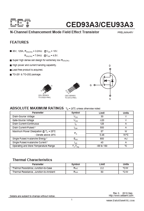
30V, 125A, RDS(ON) = 3.2mΩ @VGS = 10V. RDS(ON) = 7.0mΩ @VGS = 4.5V. Super high dense cell design for extremely low RDS(ON). High power and current handing capability. Lead free product is acquired. TO-251 & TO-252 package.
CED93A3/CEU93A3
PRELIMINARY
D G S CEU SERIES TO-252(D-PAK)
S CED SERIES TO-251(I-PAK)
ABSOLUTE MAXIMUM RATINGS
Parameter Drain-Source Voltage Gate-Source Voltage Drain Current-Continuous Drain Current-Pulsed a
Tc = 25 C unless otherwise noted Symbol Limit VDS VGS ID IDM PD EAS IAS TJ,Tstg 30
Units V V A A W W/ C m J A C
±20
125 500 57 0.46 800 40 -55 to 150
Maximum Power Dissipation @ TC = 25 C
- Derate above 25 C Single Pulsed Avalanche Energy d Single Pulsed Avalanche Current d Operating and Store Temperature Range
Thermal Characteristics
Parameter Symbol RθJC RθJA Limit 2.2 50 Units C/W C/W
.. Thermal Resistance, Junction-to-Case
Thermal Resistance, Junction-to-Ambient
Details are subject to change without notice . 1
Rev 3. 2010.Sep. http://.cetsemi.
CED93A3/CEU93A3
Electrical Characteristics
Parameter Off Characteristics Drain-Source Breakdown Voltage Zero Gate Voltage Drain Current Gate Body Leakage Current, Forward Gate Body Leakage Current, Reverse On Characteristics b Gate Threshold Voltage Static Drain-Source On-Resistance Dynamic Characteristics c Forward Transconductance Input Capacitance Output Capacitance Reverse Transfer Capacitance Switching Characteristics c Turn-On Delay Time Turn-On Rise Time Turn-Off Delay Time Turn-Off Fall Time Total Gate Charge Gate-Source Charge Gate-Drain Charge Drain-Source Diode Forward Current Drain-Source Diode Forward Voltage b td(on) tr td(off) tf Qg Qgs Qgd IS VSD VGS = 0V, IS = 20A VDS = 15V, ID = 16A, VGS = 5V VDD = 15V, ID = 1A, VGS = 10V, RGEN = 6Ω 24 19 128 72 60 12 25 125 1.5 ns ns ns ns n C n C n C A V g FS Ciss Coss Crss VDS = 10V, ID = 15A VDS = 15V, VGS = 0V, f = 1.0 MHz 50 4100 980 600 S p F p F p F VGS(th) RDS(on) VGS = VDS, ID = 250µA VGS = 10V, ID = 30A VGS =...