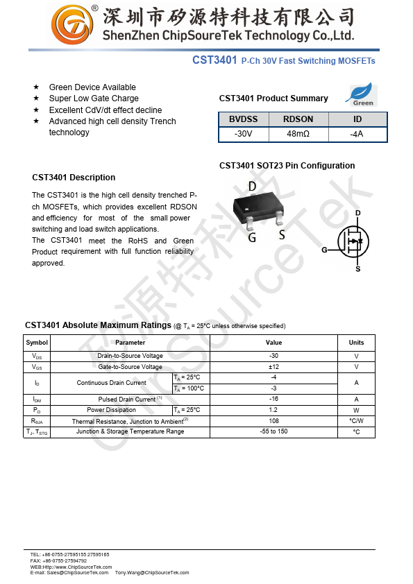
DESCRIPTION
特 rce CST3401 ABSOLUTE MAXIMUM RATINGS
(@ TA = 25°C unless otherwise specified) 源 u Symbol o VDS VGS 矽 S ID ip IDM PD RθJA Ch TJ, TSTG Parameter Drain-to-Source Voltage Gate-to-Source Voltage Continuous Drain Current Pulsed Drain Current (1) TA = 25°C TA = 100°C Power Dissipation TA = 25°C Thermal Resistance, Junction to Ambient(2) Junction & Storage Temperature Range Value -30 ±12 -4 -3 -16 1.2 108 -55 to 150 Units V V A A W °C/W °C TEL: +86-0755-27595155 27595165 FAX: +86-0755-27594792 WEB: E-mail: Sales@ChipSourceTek.com Tony.Wang@ChipSourceTek.com CST3401 P-Ch 30V Fast Switching MOSFETs CST3401 ELECTRICAL CHARACTERISTICS
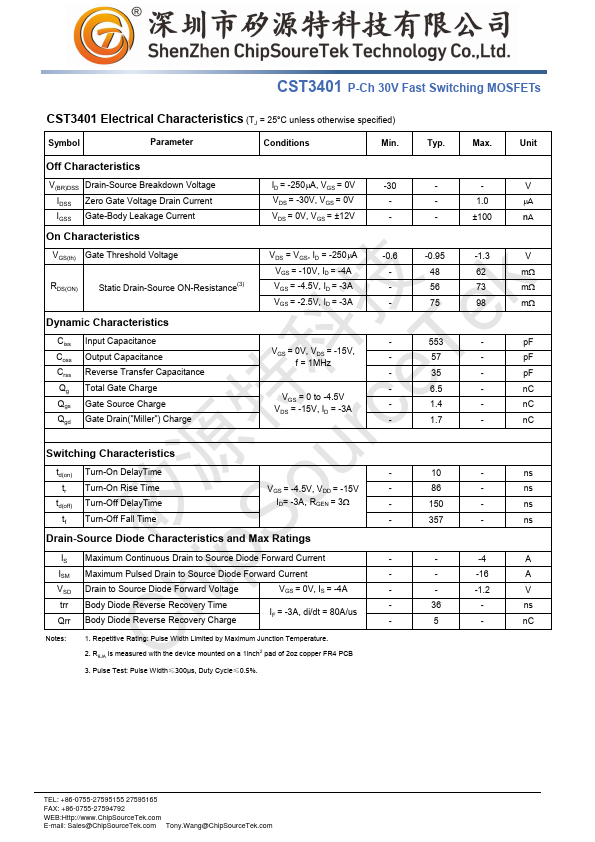
(TJ = 25°C unless otherwise specified) Symbol Parameter Conditions Min. Typ. Max. Unit Off Characteristics V(BR)DSS Drain-Source Breakdown Voltage IDSS Zero Gate Voltage Drain Current IGSS Gate-Body Leakage Current ID = -250µA, VGS = 0V -30 VDS = -30V, VGS = 0V - VDS = 0V, VGS = ±12V - - - V - 1.0 µA - ±100 nA On Characteristics VGS(th) Gate Threshold V... ChipSourceTek