ChipSourceTek PE4013SA
The PE4013SA uses advanced trench technology to provide excellent RDS(ON) and low gate charge. It can be used in a wide variety of applications.| Part No. | PE4013SA |
|---|---|
| Datasheet | PE4013SA Download |
| Manufacturer |  ChipSourceTek |
| Description | N-Channel Enhancement Mode Power MOSFET |
| Buy | Stock & Price |
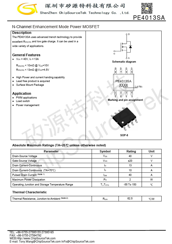
DESCRIPTION
It can be used in a wide variety of applications. PE4013SAGENERAL FEATURES
● VDS = 40V, ID = 13A RDS(ON) < 10mΩ @ VGS=10V RDS(ON) < 13mΩ @ VGS=4.5V Schematic diagram● High Power and current handing capability
● Lead free product is acquired
● Surface Mount Package Application 技
● PWM applications
● Load switch k
● Power management Marking and pin assignment 矽源特科urceTe
ABSOLUTE MAXIMUM RATINGS
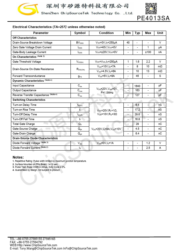
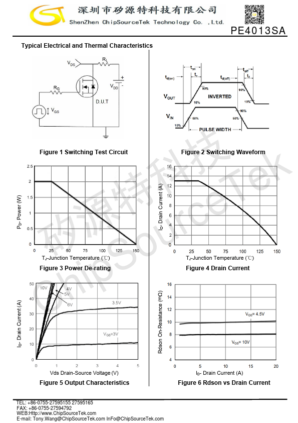
(TA=25℃ unless otherwise noted) o Parameter S Drain-Source Voltage Gate-Source Voltage ip Drain Current-Continuous Drain Current-Continuous (TA=70℃) h Pulsed Drain Current (Note 1) C Maximum Power Dissipation Symbol VDS VGS ID ID IDM PD SOP-8 Rating 40 ±20 13 10 40 2 Unit V V A A A W Operating Junction and Storage Temperature Range TJ,TSTG -55 To 150 ℃ Thermal Characteristic Thermal Resistance, Junction-to-Ambient (Note 2) RθJA 62.5 ℃/W TEL: +86-0755-27595155 27595165 FAX: +86-0755-27594792 WEB: E-mail: Tony.Wang@ChipSourceTek.com InFo@ChipSourceTek.com PE4013SA Electrical Characteri...