Datasheet Summary
MOSFET
N-Channel RoHS Device Halogen Free
Features
-Special process technology for high ESD capability. -High density cell design for extremely low RDS(ON). -Good stability and uniformity with high EAS. -Excellent package for good heat dissipation.
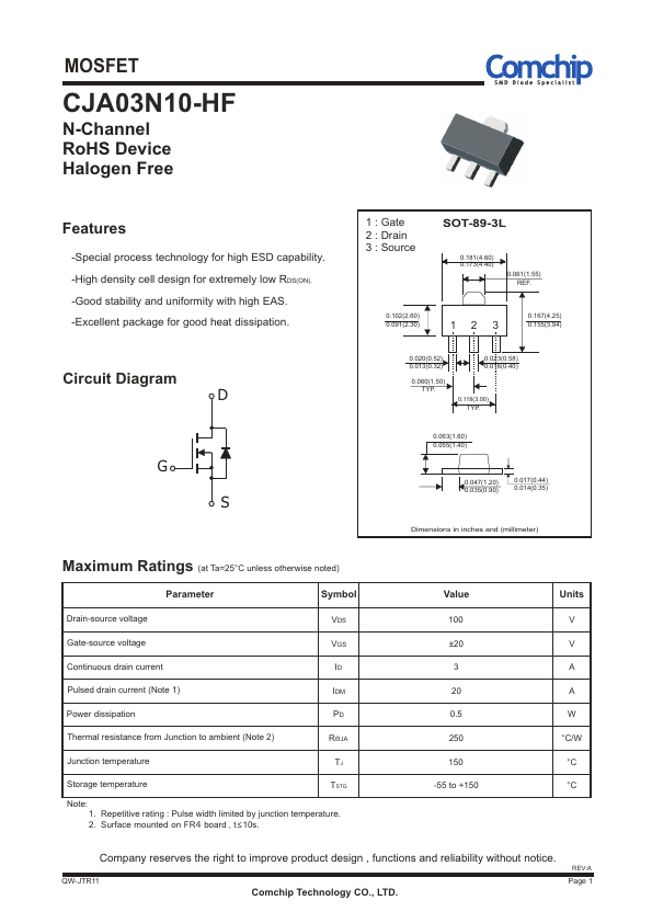
1 : Gate 2 : Drain 3 : Source
SOT-89-3L
0.181(4.60) 0.173(4.40)
0.061(1.55) REF.
0.102(2.60) 0.091(2.30)
0.167(4.25) 0.155(3.94)
Circuit Diagram
0.020(0.52) 0.013(0.32)
0.060(1.50) TYP.
0.023(0.58) 0.016(0.40)
0.118(3.00) TYP.
0.063(1.60) 0.055(1.40)
0.047(1.20) 0.035(0.90)
0.017(0.44) 0.014(0.35)
Dimensions in inches and (millimeter)
Maximum Ratings (at Ta=25°C unless otherwise noted)
Parameter
Symbol
Dr...