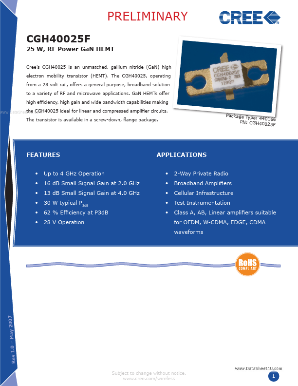
CGH40025F
CGH40025F is GaN HEMT manufactured by Cree.
FEATURES
- -
- -
- - Up to 4 GHz Operation 16 d B Small Signal Gain at 2.0 GHz 13 d B Small Signal Gain at 4.0 GHz 30 W typical P3d B 62 % Efficiency at P3d B 28 V Operation
APPLICATIONS
- -
- -
- 2-Way Private Radio Broadband Amplifiers Cellular Infrastructure Test Instrumentation Class A, AB, Linear amplifiers suitable for OFDM, W-CDMA, EDGE, CDMA waveforms
2007 Rev 1.0
- May
Subject to change without notice. .cree./wireless
Absolute Maximum Ratings (not simultaneous) at 25˚C Case Temperature
Parameter Drain-Source Voltage Gate-to-Source Voltage Storage Temperature Operating Junction Temperature Maximum Forward Gate Current Soldering Temperature Thermal Resistance, Junction to Case 1
Symbol VDSS VGS TSTG TJ IGMAX TS RθJC
Rating 84 -10, +2 -55, +150 175 4.0 245 3.8
Units Volts Volts ˚C ˚C m A ˚C ˚C/W
.. Note:
Measured for the CGH40025F at PDISS = 28 W.
Electrical Characteristics (TC = 25˚C)
Characteristics DC Characteristics2 Gate Threshold Voltage Gate Quiescent Voltage Saturated Drain Current Drain-Source Breakdown Voltage Case Operating Temperature Screw Torque VGS(th) VGS(Q) IDS VBR TC T -3.0
- 4.8 84 -10
- -2.5 -2.0 5.4 100
- - -1.8
- -
- +65 60 VDC VDC A VDC ˚C in-oz Reference 440166 Package Revision 3 VDS = 10 V, ID = 7.2 m A VDS = 28 V, ID = 250 m A VDS = 6.0 V, VGS = 2.0 V VGS = -8 V, ID = 7.2 m A Symbol Min. Typ. Max. Units Conditions
RF Characteristics (TC = 25˚C, F0 = 3.7 GHz unless otherwise noted) Small Signal Gain Power Output at 3 d B pression Drain Efficiency1 Output Mismatch Stress Dynamic Characteristics Input Capacitance Output Capacitance Feedback Capacitance CGS CDS CGD
- -
- 9.3 2.0 0.9
- -
- p F p F p F VDS = 28 V, Vgs = -8 V, f = 1 MHz VDS = 28 V, Vgs = -8 V, f = 1 MHz VDS = 28 V, Vgs = -8 V, f = 1 MHz GSS P3d B
η
- -
- -
13 30 62 TBD
- -
- - d B W % Y
VDD = 28 V, IDQ = 250 m A VDD = 28 V, IDQ = 250 m A VDD = 28 V, IDQ = 250 m A, P3d B No damage at all phase angles, VDD = 28 V, IDQ = 250 m A, POUT = 12 W...