FEATURES
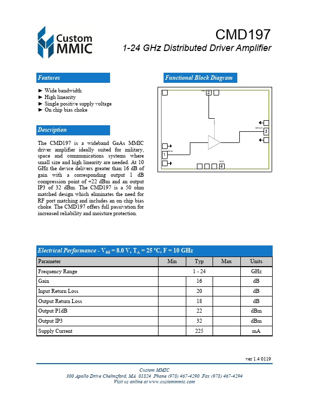
► Wide bandwidth ► High linearity ► Single positive supply voltage ► On chip bias choke DESCRIPTION
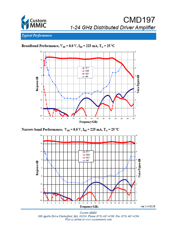
At 10 GHz the device delivers greater than 16 dB of gain with a corresponding output 1 dB compression point of +22 dBm and an output IP3 of 32 dBm. Functional Block Diagram 2Vdd RFIN 1 ACG 4 RFOUT 3 Electrical Performance - Vdd = 8.0 V, TA = 25 oC, F = 10 GHz Parameter Min Typ Frequency Range 1 - 24 Gain 16 Input Return Loss 20 Output Return Loss 18 Output P1dB 22 Output IP3 32 Supply Current 225 Max Units GHz dB dB dB dBm dBm mA ver 1.4 011