CY2509
CY2509 is Ten/Eleven Output Zero Delay Buffer manufactured by Cypress.
- Part of the CY2510 comparator family.
- Part of the CY2510 comparator family.
CY2509/10
Spread Aware™, Ten/Eleven Output Zero Delay Buffer
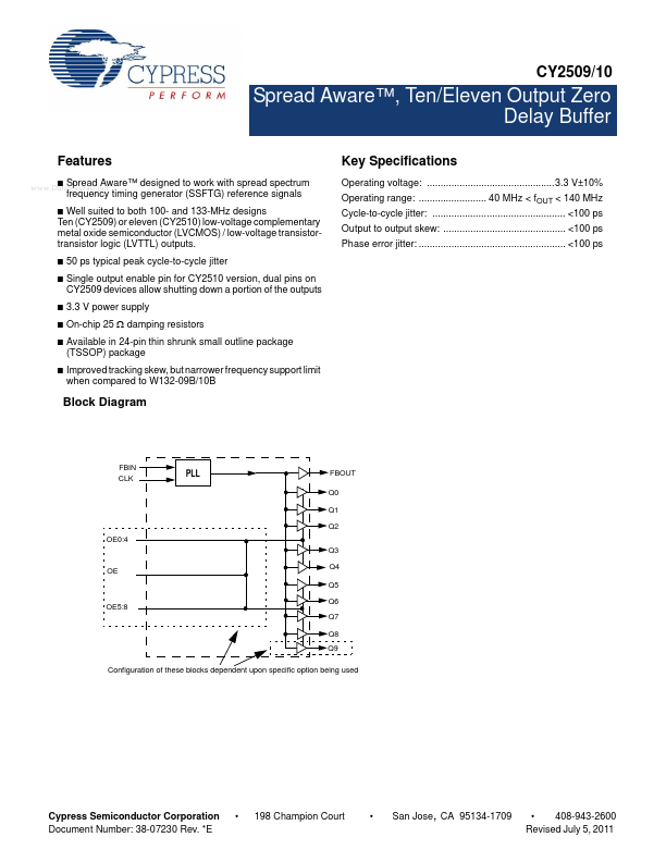
Features
- Spread Aware™ ..net
- Key Specifications
Operating voltage: ...............................................3.3 V±10% Operating range: ......................... 40 MHz < fOUT < 140 MHz Cycle-to-cycle jitter: ................................................. <100 ps Output to output skew: ............................................. <100 ps Phase error jitter: ...................................................... <100 ps designed to work with spread spectrum frequency timing generator (SSFTG) reference signals
Well suited to both 100- and 133-MHz designs Ten (CY2509) or eleven (CY2510) low-voltage...