CY25103
CY25103 is Programmable Spread Spectrum Clock Generator manufactured by Cypress.
..
Programmable Spread Spectrum Clock Generator for EMI Reduction
Description
This document describes the programmed values and functions of CY25103. Refer to the CY25100 data sheet for detailed product description and specifications.
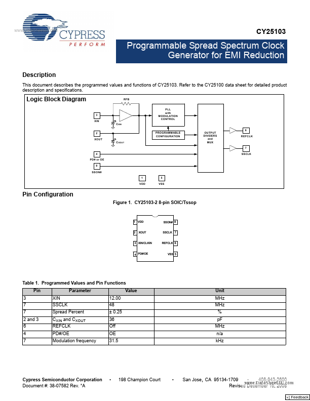
Logic Block Diagram
3 XIN C XIN 2 XOUT
PLL with MODULATION CONTROL
PROGRAMMABLE CONFIGURATION C XOUT
OUTPUT DIVIDERS and MUX
6 REFCLK
7 4 PD# or OE 8 SSON# 1 VDD 5 VSS SSCLK
Pin Configuration
Figure 1. CY25103-2 8-pin SOIC/Tssop
1 VDD 2 XOUT
SSON# 8 SSCLK 7 REFCLK 6
3 XIN/CLKIN 4 PD#/OE
VSS 5
Table 1. Programmed Values and Pin Functions Pin 3 7 7 2 and 3 6 4 7 XIN SSCLK Spread Percent CXIN and CXOUT REFCLK PD#/OE...