CY2CC1810
CY2CC1810 is 1:10 Clock Fanout Buffer manufactured by Cypress.
CY2CC810
1:10 Clock Fanout Buffer
Features
- Low-voltage operation
- VDD range from 2.5 V to 3.3 V
- 1:10 fanout
- Over voltage tolerant input hot swappable
- Drives either a 50-Ohm or 75-Ohm transmission line
- Low-input capacitance
- 250 ps typical output-to-output skew
- 19 ps typical DJ jitter
- Typical propagation delay < 3.5 ns
- High-speed operation > 500 MHz
- Industrial temperature range
- Available packages include: SSOP
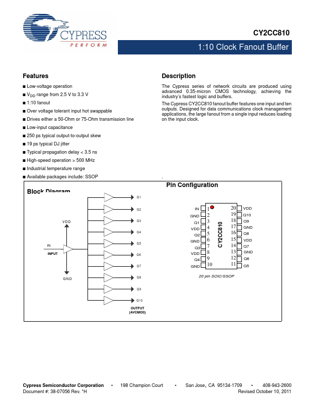
Block Diagram
IN INPUT
Q1
Q2 Q3 Q4 Q5 Q6 Q7 Q8 Q9 Q10 OUTPUT (AVCMOS)
Description
The Cypress series of network circuits are produced using advanced 0.35-micron CMOS technology, achieving the industry’s fastest logic and buffers.
The Cypress CY2CC810...