CY2CP1504
CY2CP1504 is 1:4 LVCMOS to LVPECL Fanout Buffer manufactured by Cypress.
1:4 LVCMOS to LVPECL Fanout Buffer with Selectable Clock Input
1:4 LVCMOS to LVPECL Fanout Buffer with Selectable Clock Input
Features
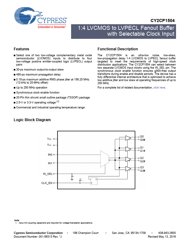
- Select one of two low-voltage plementary metal oxide semiconductor (LVCMOS) inputs to distribute to four low-voltage positive emitter-coupled logic (LVPECL) output pairs
- 30-ps maximum output-to-output skew
- 480-ps maximum propagation delay
- 0.15-ps maximum additive RMS phase jitter at 156.25 MHz
(12-kHz to 20-MHz offset)
- Up to 250 MHz operation
- Synchronous clock enable function
- 20-Pin thin shrunk small outline package (TSSOP) package
- 2.5-V or 3.3-V operating voltage [1]
- mercial and industrial operating temperature...