CY62256V
Features
- -
- -
- -
- - 55, 70 ns access time CMOS for optimum speed/power Wide voltage range: 2.7V- 3.6V Low active power (70 ns, LL version)
- 108 m W (max.) Low standby power (70 ns, LL version)
- 18 µW (max.) Easy memory expansion with CE and OE features
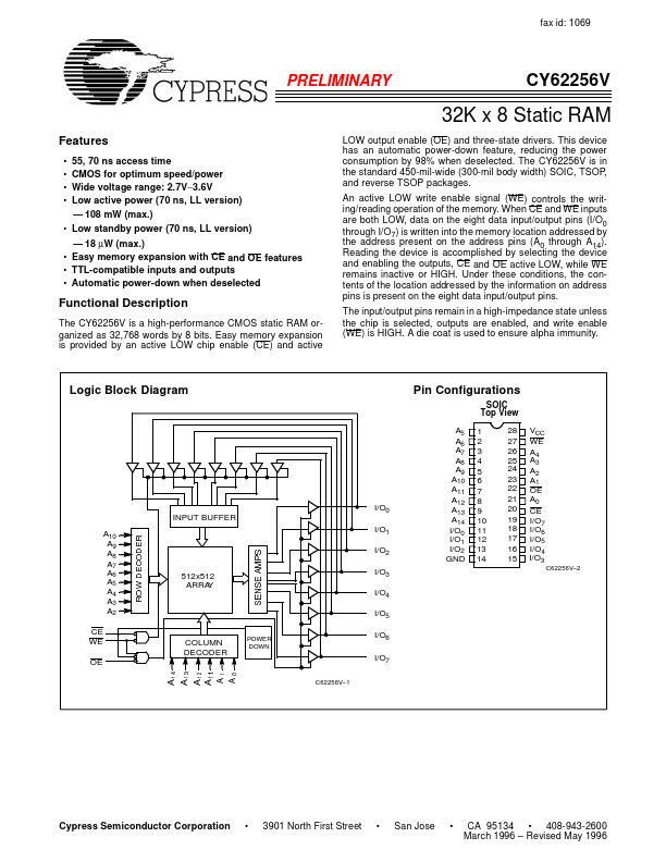
TTL-patible inputs and outputs Automatic power-down when deselected LOW output enable (OE) and three-state drivers. This device has an automatic power-down feature
, reducing the power consumption by 98% when deselected. The CY62256V is in the standard 450-mil-wide (300-mil body width) SOIC, TSOP, and reverse TSOP packages. An active LOW write enable signal (WE) controls the writing/reading operation of the memory. When CE and WE inputs are both LOW, data on the eight data input/output pins (I/O0 through I/O7) is written into the memory location addressed by the address present on the address pins (A0 through A14). Reading the device is acplished by selecting the device and enabling the outputs, CE and OE active LOW, while WE...