CY7C09289V
Key Features
- True dual-ported memory cells that allow simultaneous access of the same memory location
- Six flow through/pipelined devices: ❐ 16K × 16 / 18 organization (CY7C09269V/369V) ❐ 32K × 16 organization (CY7C09279V) ❐ 64K × 16 / 18 organization (CY7C09289V/389V)
- Three modes: ❐ Flow through ❐ Pipelined ❐ Burst
- Pipelined output mode on both ports allows fast 100 MHz operation
- 0.35 micron CMOS for optimum speed and power
- High speed clock to data access: 7.5[1], 9, 12 ns (max)
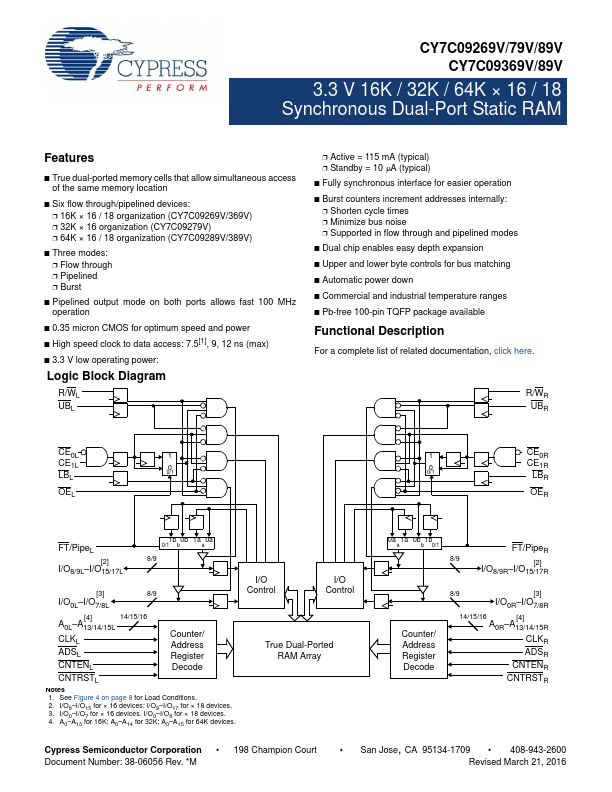
- 3.3 V low operating power: Logic Block Diagram R/WL UBL ❐ Active = 115 mA (typical) ❐ Standby = 10 A (typical)
- Fully synchronous interface for easier operation
- Burst counters increment addresses internally: ❐ Shorten cycle times ❐ Minimize bus noise ❐ Supported in flow through and pipeli