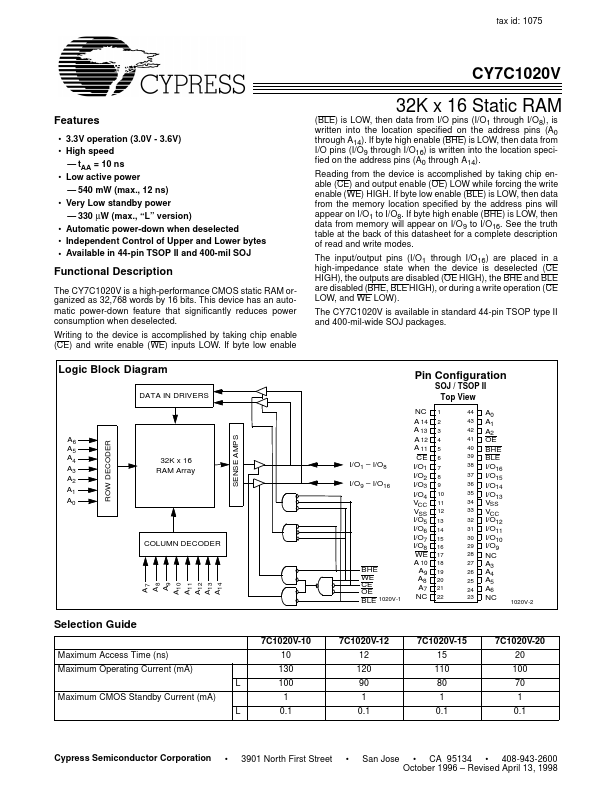
CY7C1020V
Overview
- 3.3V operation (3.0V - 3.6V)
- High speed - tAA = 10 ns
- Low active power - 540 mW (max., 12 ns)
- Very Low standby power - 330 µW (max., “L” version)
- Automatic power-down when deselected
- Independent Control of Upper and Lower bytes
- Available in 44-pin TSOP II and 400-mil SOJ (BLE) is LOW, then data from I/O pins (I/O1 through I/O8), is written into the location specified on the address pins (A0 through A14). If byte high enable (BHE) is LOW, then data from I/O pins (I/O9 through I/O16) is written into the location specified on the address pins (A0 through A14). Reading from the device is accomplished by taking chip enable (CE) and output enable (OE) LOW while forcing the write enable (WE) HIGH. If byte low enable (BLE) is LOW, then data from the memory location specified by the address pins will appear on I/O1 to I/O8. If byte high enable (BHE) is LOW, then data from memory will appear on I/O 9 to I/O16. See the truth table at the back of this datasheet for a complete description of read and write modes. The input/output pins (I/O1 through I/O16) are placed in a high-impedance state when the device is deselected (CE HIGH), the outputs are disabled (OE HIGH), the BHE and BLE are disabled (BHE, BLE HIGH), or during a write operation (CE LOW, and WE LOW). The CY7C1020V is available in standard 44-pin TSOP type II and 400-mil-wide SOJ packages. Functional Description The CY7C1020V is a high-performance CMOS static RAM organized as 32,768 words by 16 bits. This device has an automatic power-down feature that significantly reduces power consumption when deselected. Writing to the device is accomplished by taking chip enable (CE) and write enable (WE) inputs LOW. If byte low enable Logic Block Diagram