CY7C1022
CY7C1022 is 32K x 16 Static RAM manufactured by Cypress.
022CY7C10
..
PRELIMINARY
32K x 16 Static RAM
Features
- 5.0V operation (± 10%)
- High speed
- tAA = 12 ns
- Low active power
- 825 mW (max., 10 ns, “L” version)
- Very Low standby power
- 500 µW (max., “L” version)
- Automatic power-down when deselected
- Independent Control of Upper and Lower bytes
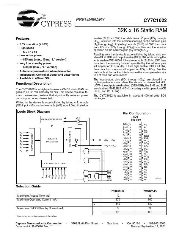
- Available in 400-mil SOJ enable (BLE) is LOW, then data from I/O pins (I/O1 through I/O8), is written into the location specified on the address pins (A0 through A14). If byte high enable (BHE) is LOW, then data from I/O pins (I/O9 through I/O16) is written into the location specified on the address pins (A0 through A14). Reading from the device is acplished...