CY7C1302CV25
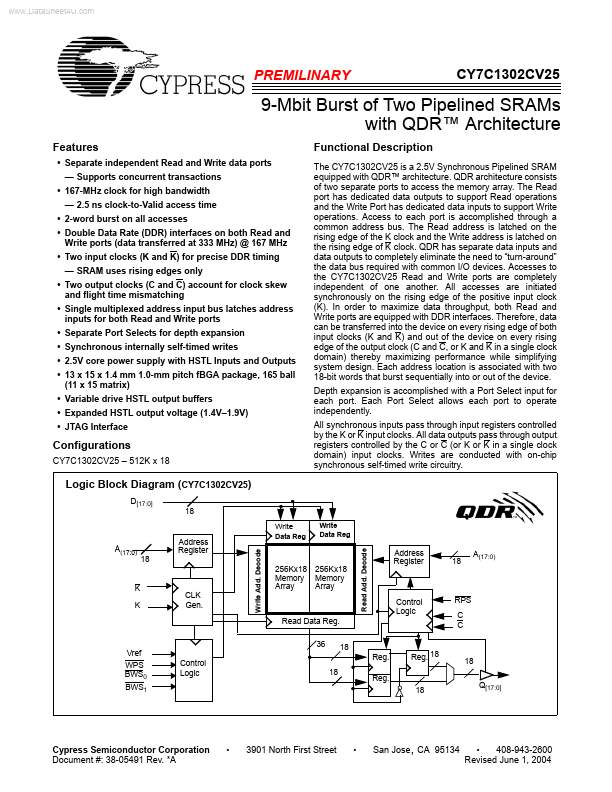
Overview
- Separate independent Read and Write data ports - Supports concurrent transactions
- 167-MHz clock for high bandwidth - 2.5 ns clock-to-Valid access time
- 2-word burst on all accesses
- Double Data Rate (DDR) interfaces on both Read and Write ports (data transferred at 333 MHz) @ 167 MHz
- Two input clocks (K and K) for precise DDR timing - SRAM uses rising edges only
- Two output clocks (C and C) account for clock skew and flight time mismatching
- Single multiplexed address input bus latches address inputs for both Read and Write ports
- Separate Port Selects for depth expansion
- Synchronous internally self-timed writes
- 2.5V core power supply with HSTL Inputs and Outputs