Datasheet Summary
..
PRELIMINARY
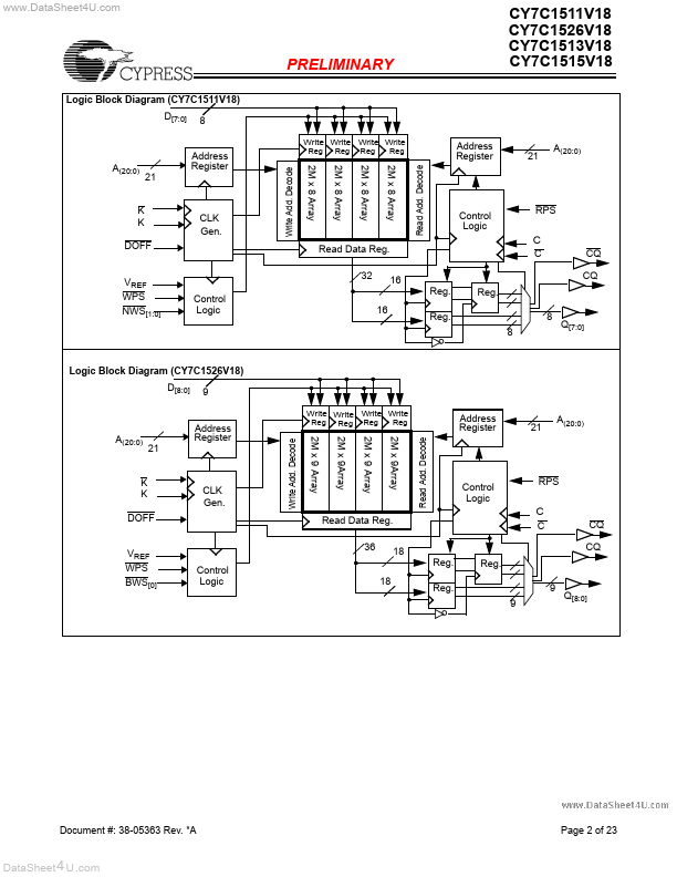
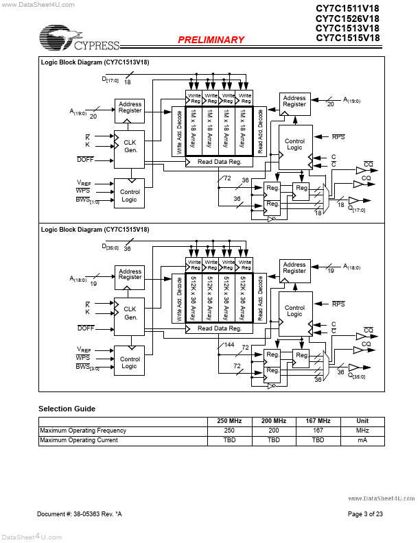
CY7C1511V18 CY7C1526V18 CY7C1513V18 CY7C1515V18
72-Mbit QDR™-II SRAM 4-Word Burst Architecture
Features
- Separate Independent Read and Write Data Ports
- Supports concurrent transactions
- 250-MHz Clock for High Bandwidth
- 4-Word Burst for reducing address bus frequency
- Double Data Rate (DDR) interfaces on both Read and Write Ports (data transferred at 500 MHz) at 250 MHz
- Two input clocks (K and K) for precise DDR timing
- SRAM uses rising edges only
- Two output clocks (C and C) accounts for clock skew and flight time mismatching
- Echo clocks (CQ and CQ) simplify data capture in high speed systems
- Single multiplexed address input bus latches...