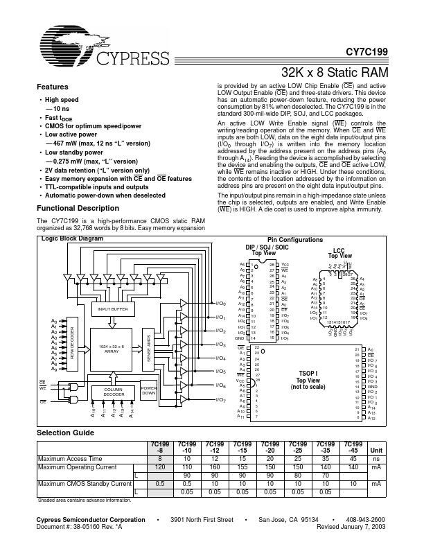
• Part: CY7C199
  • Description: 32K x 8 Static RAM
  • Manufacturer: Cypress
  • Size: 317.03 KB
Download CY7C199 Datasheet PDF
Cypress
CY7C199
CY7C199 is 32K x 8 Static RAM manufactured by Cypress.
- Part of the CY7 comparator family.
32K x 8 Static RAM Features - High speed - 10 ns - Fast t DOE - CMOS for optimum speed/power - Low active power - 467 m W (max, 12 ns “L” version) - Low standby power - 0.275 m W (max, “L” version) - 2V data retention (“L” version only) - Easy memory expansion with CE and OE Features - TTL-patible inputs and outputs - Automatic power-down when deselected is provided by an active LOW Chip Enable (CE) and active LOW Output Enable (OE) and three-state drivers. This device has an automatic power-down feature, reducing the power consumption by 81% when deselected. The CY7C199 is in the standard 300-mil-wide DIP, SOJ, and LCC packages. An active LOW Write Enable signal (WE) controls the writing/reading operation of the memory. When CE and WE inputs are both LOW, data on the eight data input/output pins (I/O0 through I/O7) is written into the memory location addressed by the address present on the address pins (A0 through A14). Reading the device is acplished by selecting the device and enabling the outputs, CE and OE active LOW, while WE remains inactive or HIGH. Under these conditions, the contents of the location addressed by the information on address pins are present on the eight data input/output pins. The input/output pins remain in a high-impedance state unless the chip is selected, outputs are enabled, and Write Enable (WE) is HIGH. A die coat is used to improve alpha immunity. Functional Description The CY7C199 is a high-performance CMOS static RAM organized as 32,768 words by 8 bits. Easy memory expansion Logic Block Diagram Pin Configurations DIP / SOJ / SOIC Top View A5 A6 A7 A8 A9 A10 A11 A12 A13 A14 I/O0 I/O1 I/O2 GND 1 2 3 4 5 6 7 8 9 10 11 12 13 14 22 23 24 25 26 27 28 1 2 3 4 5 6 7 LCC Top View 3 2 1 28 27 4 26 A4 5 25 A3 6 24 A2 7 23 A1 8 22 OE 9 21 A0 20 CE 10 11 19 I/O7 18 I/O6 12 1314151617 I/O2 GND I/O3 I/O4 I/O5 A7 A6 A5 VCC WE A8 A9 A10 A11 A12 A13 A14 I/O0 I/O1 I/O0 INPUT BUFFER A0 A1 A2 A3 A4 A5 A6 A7 A8 A9 CE WE OE I/O1 ROW...