CY7C4255
CY7C4255 is 8K/16Kx18 Deep Sync FIFOs manufactured by Cypress.
1CY 7C42 65 fax id: 5413
PRELIMINARY
CY7C4255 CY7C4265
8K/16Kx18 Deep Sync FIFOs
Features
- High-speed, low-power, first-in first-out (FIFO) memories
- 8K x 18 (CY7C4255)
- 16K x 18 (CY7C4265)
- 0.5 micron CMOS for optimum speed/power
- High-speed 100-MHz operation (10 ns read/write cycle times)
- Low power
- ICC=45 m A
- Fully asynchronous and simultaneous read and write operation
- Empty, Full, Half Full, and programmable Almost Empty and Almost Full status flags
- TTL patible
- Retransmit function
- Output Enable (OE) pins
- Independent read and write enable pins
- Center power and ground pins for reduced noise
- Supports free-running 50% duty cycle clock inputs
- Width Expansion Capability
- Depth Expansion Capability
- 64-pin PLCC and 64-pin TQFP
- Pin-patible density upgrade to CY7C42X5 family
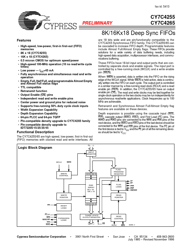
- Pin-patible density upgrade to IDT72205/15/25/35/45 are 18 bits wide and are pin/functionally patible to the CY7C42X5 Synchronous FIFO family. The CY7C4255/65 can be cascaded to increase FIFO depth. Programmable Features include Almost Full/Almost Empty flags. These FIFOs provide solutions for a wide variety of data buffering needs, including high-speed data acquisition, multiprocessor interfaces, and munications buffering. These FIFOs have 18-bit input and output ports that are controlled by separate clock and enable signals. The input port is controlled by a free-running clock (WCLK) and a write enable pin (WEN). When WEN is asserted, data is written into the FIFO on the rising edge of the WCLK signal. While WEN is held active, data is continually written into the FIFO on each cycle. The output port is controlled in a similar manner by a free-running read clock (RCLK) and a read enable pin (REN). In addition, the CY7C4255/65 have an output enable pin (OE). The read and write clocks may be tied together for single-clock operation or the two clocks may be run independently for asynchronous read/write applications. Clock frequencies up to 100 MHz are...