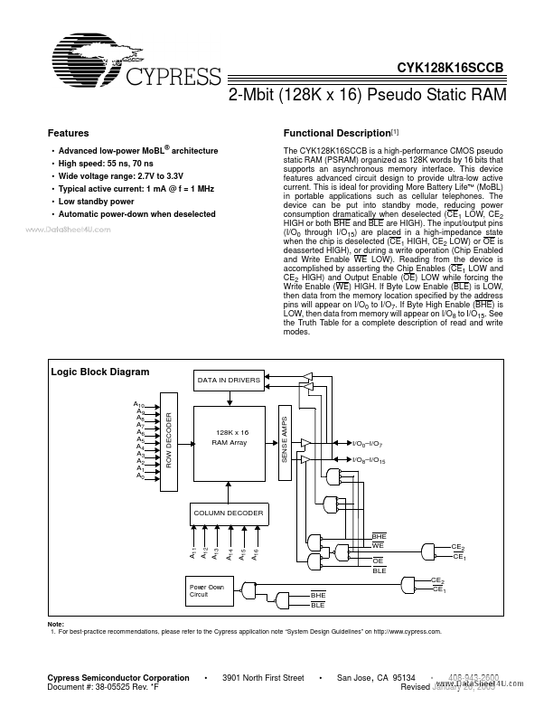
CYK128K16SCCB
CYK128K16SCCB is 2-Mbit (128K x 16) Pseudo Static RAM manufactured by Cypress.
2-Mbit (128K x 16) Pseudo Static RAM
Features
- Advanced low-power Mo BL® architecture
- High speed: 55 ns, 70 ns
- Wide voltage range: 2.7V to 3.3V
- Typical active current: 1 m A @ f = 1 MHz
- Low standby power
- Automatic power-down when deselected
..
Functional Description[1]
The CYK128K16SCCB is a high-performance CMOS pseudo static RAM (PSRAM) organized as 128K words by 16 bits that supports an asynchronous memory interface. This device Features advanced circuit design to provide ultra-low active current. This is ideal for providing More Battery Life™ (Mo BL) in portable applications such as cellular telephones. The device can be put into standby mode, reducing power consumption dramatically when deselected (CE1 LOW, CE2 HIGH or both BHE and BLE are HIGH). The input/output pins (I/O0 through I/O15) are placed in a high-impedance state when the chip is deselected (CE1 HIGH, CE2 LOW) or OE is deasserted HIGH), or during a write operation (Chip Enabled and Write Enable WE LOW). Reading from the device is acplished by asserting the Chip Enables (CE1 LOW and CE2 HIGH) and Output Enable (OE) LOW while forcing the Write Enable (WE) HIGH. If Byte Low Enable (BLE) is LOW, then data from the memory location specified by the address pins will appear on I/O0 to I/O7. If Byte High Enable (BHE) is LOW, then data from memory will appear on I/O8 to I/O15. See the Truth Table for a plete description of read and write modes.
Logic Block Diagram
A10 A9 A8 A7 A6 A5 A4 A3 A2 A1 A0
DATA IN DRIVERS
ROW DECODER
128K x 16 RAM Array
SENSE AMPS
I/O0- I/O7 I/O8- I/O15
COLUMN DECODER BHE WE OE BLE BHE BLE CE2 CE1
CE2 CE1
A11
A12
A13
A14
A15
Pow er Down Circuit
Note: 1. For best-practice remendations, please refer to the Cypress application note “System Design Guidelines” on http://.cypress..
A16
Cypress Semiconductor Corporation Document #: 38-05525 Rev.
-...